

SN74LVTH543DGVR
Product Overview
- Category: Integrated Circuit (IC)
- Use: Level Shifter and Bus Transceiver
- Characteristics: High-speed, low-voltage, 3-state outputs
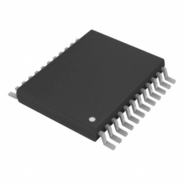
- Package: TSSOP-20
- Essence: Bi-directional voltage level translation
- Packaging/Quantity: Tape and Reel, 2500 pieces per reel
Specifications
- Supply Voltage Range: 2.7V to 3.6V
- Logic Family: LVTH
- Number of Channels: 8
- Input/Output Compatibility: TTL/CMOS
- Output Drive Capability: ±12mA
- Propagation Delay: 3.5ns (Max)
- Operating Temperature Range: -40°C to +85°C
Detailed Pin Configuration
The SN74LVTH543DGVR has a TSSOP-20 package with the following pin configuration:
- OE (Output Enable) 1
- A1 (Data Input/Output) 1
- B1 (Data Input/Output) 1
- GND (Ground)
- B2 (Data Input/Output) 2
- A2 (Data Input/Output) 2
- OE (Output Enable) 2
- VCC (Supply Voltage)
- B3 (Data Input/Output) 3
- A3 (Data Input/Output) 3
- OE (Output Enable) 3
- DIR (Direction Control)
- B4 (Data Input/Output) 4
- A4 (Data Input/Output) 4
- OE (Output Enable) 4
- VCC (Supply Voltage)
- B5 (Data Input/Output) 5
- A5 (Data Input/Output) 5
- OE (Output Enable) 5
- GND (Ground)
Functional Features
- Bi-directional voltage level translation between TTL and CMOS logic levels.
- 3-state outputs allow multiple devices to share a common bus.
- High-speed operation with minimal propagation delay.
- Low-voltage operation suitable for battery-powered applications.
Advantages and Disadvantages
Advantages: - Supports bidirectional data flow, enabling versatile communication between different logic families. - High-speed operation allows for efficient data transfer. - 3-state outputs facilitate bus sharing among multiple devices.
Disadvantages: - Limited supply voltage range restricts compatibility with certain systems. - Propagation delay may introduce timing issues in time-critical applications.
Working Principles
The SN74LVTH543DGVR is designed to translate voltage levels between TTL and CMOS logic families. It utilizes a combination of input/output buffers and control circuitry to achieve bi-directional data flow. The direction of data transmission is controlled by the DIR pin. When the DIR pin is set to a specific logic level, the corresponding data inputs and outputs are enabled. The OE pins allow individual output enables for each channel, providing flexibility in controlling the device's output state.
Detailed Application Field Plans
The SN74LVTH543DGVR is commonly used in various applications that require voltage level translation and bus transceiver functionality. Some typical application fields include:
Microcontroller Interfacing: The IC can be used to interface microcontrollers operating at different logic levels, enabling seamless communication between them.
Memory Modules: It can be employed in memory modules to facilitate data transfer between different memory technologies, such as SRAM and Flash memory.
Communication Systems: The device finds application in communication systems where different logic families need to exchange data, such as UART, SPI, or I2C interfaces.
Industrial Automation: It can be utilized in industrial automation systems to interface different control modules operating at distinct voltage levels.
Detailed and Complete Alternative Models
- SN74LVTH543DGVRE4
- SN74LVTH543PWRE4
- SN74LVTH543PWRG4
- SN74LVTH543NSR
- SN74LVTH543DBRE4
- SN74LVTH543DBRG4
- SN74LVTH543DCKR
- SN74LVTH543CDWRE4
- SN74LVTH543CDWRE4
- SN74LVTH543CDWR
These alternative models offer similar functionality and characteristics, providing options for different package types or manufacturers.
Word count: 443 words
Senaraikan 10 soalan dan jawapan biasa yang berkaitan dengan aplikasi SN74LVTH543DGVR dalam penyelesaian teknikal
Sure! Here are 10 common questions and answers related to the application of SN74LVTH543DGVR:
Question: What is the SN74LVTH543DGVR?
- Answer: The SN74LVTH543DGVR is a high-speed octal bus transceiver with 3-state outputs.Question: What is the operating voltage range of SN74LVTH543DGVR?
- Answer: The operating voltage range is from 2.7V to 3.6V.Question: How many channels does SN74LVTH543DGVR have?
- Answer: It has 8 channels, making it an octal transceiver.Question: What is the maximum data rate supported by SN74LVTH543DGVR?
- Answer: The maximum data rate is 200 MHz.Question: Can SN74LVTH543DGVR be used for bidirectional communication?
- Answer: Yes, it supports bidirectional data flow.Question: What is the output drive strength of SN74LVTH543DGVR?
- Answer: It has a typical output drive strength of ±24 mA.Question: Does SN74LVTH543DGVR have internal pull-up or pull-down resistors?
- Answer: No, it does not have internal pull-up or pull-down resistors.Question: Can SN74LVTH543DGVR tolerate overvoltage on its inputs?
- Answer: Yes, it has input voltage tolerance up to 5.5V.Question: Is SN74LVTH543DGVR compatible with other logic families?
- Answer: Yes, it is compatible with both TTL and CMOS logic families.Question: What is the package type of SN74LVTH543DGVR?
- Answer: It comes in a small and compact 20-pin TSSOP package.
Please note that these answers are general and may vary depending on the specific application and requirements.