

SN74LVCH244ARGYRG4
Product Overview
- Category: Integrated Circuit (IC)
- Use: Buffer/Line Driver
- Characteristics: Low-Voltage, High-Speed, Octal Bus Buffer with 3-State Outputs
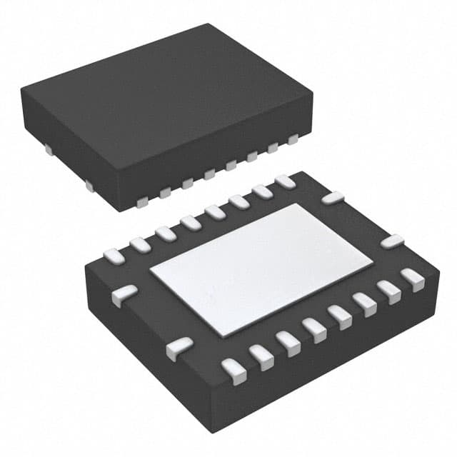
- Package: VQFN-20
- Essence: This IC is designed to provide buffering and line driving capabilities for digital signals in low-voltage applications.
- Packaging/Quantity: Available in reels of 2500 units.
Specifications
- Supply Voltage Range: 1.65V to 3.6V
- Input Voltage Range: 0V to VCC
- Output Voltage Range: 0V to VCC
- Maximum Operating Frequency: 200MHz
- Number of Channels: 8
- Output Drive Capability: ±24mA
- Propagation Delay: 2.5ns (Max)
- Operating Temperature Range: -40°C to +85°C
Detailed Pin Configuration
The SN74LVCH244ARGYRG4 has a total of 20 pins, which are assigned as follows:
- A1 - Input/Output
- Y1 - Output
- A2 - Input/Output
- Y2 - Output
- GND - Ground
- Y3 - Output
- A3 - Input/Output
- Y4 - Output
- VCC - Power Supply
- OE - Output Enable
- A4 - Input/Output
- Y5 - Output
- A5 - Input/Output
- Y6 - Output
- GND - Ground
- Y7 - Output
- A6 - Input/Output
- Y8 - Output
- VCC - Power Supply
- GND - Ground
Functional Features
- Low-voltage operation allows compatibility with a wide range of digital systems.
- High-speed performance enables efficient signal buffering and line driving.
- 3-state outputs provide flexibility in controlling the output state.
- Octal bus buffer design allows for easy interfacing with multiple devices.
Advantages and Disadvantages
Advantages: - Wide supply voltage range enables compatibility with various systems. - High-speed operation ensures efficient signal transmission. - 3-state outputs allow for flexible control of the output state. - Octal bus buffer design simplifies system integration.
Disadvantages: - Limited number of channels (8) may not be sufficient for certain applications requiring more inputs/outputs. - Propagation delay of 2.5ns (Max) may introduce timing issues in high-frequency applications.
Working Principles
The SN74LVCH244ARGYRG4 operates by receiving digital input signals on its input pins (A1-A6) and providing buffered output signals on its corresponding output pins (Y1-Y8). The output enable pin (OE) controls the state of the outputs, allowing them to be either active or in a high-impedance state.
When the OE pin is low, the outputs are enabled and actively driven according to the input signals. Conversely, when the OE pin is high, the outputs enter a high-impedance state, effectively disconnecting them from the rest of the circuit.
Detailed Application Field Plans
The SN74LVCH244ARGYRG4 can be used in various applications, including but not limited to:
Microprocessor/Controller Interfacing: The IC can be employed to interface microprocessors or controllers with other peripheral devices, ensuring proper signal buffering and line driving.
Data Communication Systems: It can be utilized in data communication systems to enhance signal integrity and reduce noise interference during data transmission.
Memory Modules: The IC can be integrated into memory modules to facilitate data transfer between the memory and other components of a system.
Industrial Automation: It finds applications in industrial automation systems where reliable signal buffering and line driving are crucial for efficient operation.
Detailed and Complete Alternative Models
- SN74LVCH244A: Similar to SN74LVCH244ARGYRG4, but available in different package options.
- SN74LVC244A: Low-voltage octal buffer with 3-state outputs, suitable for similar applications.
- SN74LVTH244A: Low-voltage octal buffer/line driver with 3-state outputs, designed for high-speed applications.
These alternative models offer similar functionality and characteristics, providing flexibility in choosing the most suitable option for specific requirements.
Word count: 536 words
Senaraikan 10 soalan dan jawapan biasa yang berkaitan dengan aplikasi SN74LVCH244ARGYRG4 dalam penyelesaian teknikal
What is the operating voltage range of SN74LVCH244ARGYRG4?
- The operating voltage range of SN74LVCH244ARGYRG4 is 1.65V to 3.6V.What is the maximum input current of SN74LVCH244ARGYRG4?
- The maximum input current of SN74LVCH244ARGYRG4 is ±50mA.Can SN74LVCH244ARGYRG4 be used for level shifting applications?
- Yes, SN74LVCH244ARGYRG4 can be used for level shifting applications due to its wide operating voltage range.What is the typical propagation delay of SN74LVCH244ARGYRG4?
- The typical propagation delay of SN74LVCH244ARGYRG4 is 3.5ns.Is SN74LVCH244ARGYRG4 suitable for use in automotive applications?
- Yes, SN74LVCH244ARGYRG4 is suitable for use in automotive applications as it is AEC-Q100 qualified.Can SN74LVCH244ARGYRG4 be used in bidirectional data transfer applications?
- Yes, SN74LVCH244ARGYRG4 can be used in bidirectional data transfer applications as it has non-inverting outputs.What is the maximum operating frequency of SN74LVCH244ARGYRG4?
- The maximum operating frequency of SN74LVCH244ARGYRG4 is 80MHz.Does SN74LVCH244ARGYRG4 have overvoltage-tolerant inputs?
- Yes, SN74LVCH244ARGYRG4 has overvoltage-tolerant inputs up to 5.5V.Can SN74LVCH244ARGYRG4 be used in battery-powered applications?
- Yes, SN74LVCH244ARGYRG4 can be used in battery-powered applications due to its low power consumption.Is SN74LVCH244ARGYRG4 available in a small form factor package?
- Yes, SN74LVCH244ARGYRG4 is available in a small 20-pin VQFN package for space-constrained applications.