

SN74LVC540ADGVR
Product Overview
- Category: Integrated Circuit (IC)
- Use: Logic Level Shifter
- Characteristics: Low Voltage, CMOS Technology
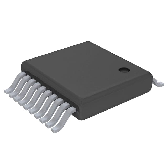
- Package: VSSOP (Very Small Outline Package)
- Essence: Bidirectional Octal Buffer/Line Driver with 3-State Outputs
- Packaging/Quantity: Tape and Reel, 2500 pieces per reel
Specifications
The SN74LVC540ADGVR is an integrated circuit belonging to the logic level shifter category. It is designed to shift signals from one voltage level to another, making it suitable for interfacing between different logic families or devices operating at different voltage levels. The IC operates on low voltage and utilizes CMOS technology, ensuring efficient power consumption and high noise immunity.
Detailed Pin Configuration
The SN74LVC540ADGVR features a 20-pin VSSOP package. The pin configuration is as follows:
- OE (Output Enable) - Output control pin
- A1-A8 - Input/output pins for data signals
- GND - Ground reference
- B1-B8 - Input/output pins for data signals
- VCC - Power supply voltage
- DIR (Direction Control) - Direction control pin
Functional Features
- Bidirectional Buffer/Line Driver: The SN74LVC540ADGVR can function as both a buffer and a line driver, allowing bidirectional signal transmission.
- 3-State Outputs: The IC offers 3-state outputs, enabling the connection of multiple devices without causing conflicts.
- High-Speed Operation: With its CMOS technology, the IC provides fast switching speeds, making it suitable for high-speed applications.
- Wide Operating Voltage Range: The SN74LVC540ADGVR supports a wide range of operating voltages, enhancing its compatibility with various systems.
Advantages and Disadvantages
Advantages: - Efficient Power Consumption: The IC operates on low voltage, resulting in reduced power consumption. - Noise Immunity: CMOS technology provides high noise immunity, ensuring reliable signal transmission. - Bidirectional Functionality: The ability to function as both a buffer and a line driver offers flexibility in signal routing.
Disadvantages: - Limited Voltage Range: The IC may not be suitable for applications requiring voltage shifting beyond its specified range. - Sensitivity to ESD: Like most integrated circuits, the SN74LVC540ADGVR is sensitive to electrostatic discharge (ESD) and requires proper handling during installation.
Working Principles
The SN74LVC540ADGVR utilizes a combination of MOSFETs and CMOS technology to achieve logic level shifting. When the direction control pin (DIR) is set to a specific state, the IC either buffers or drives the input signals based on the desired voltage level conversion. The output enable pin (OE) allows the user to control the output state, enabling or disabling signal transmission.
Detailed Application Field Plans
The SN74LVC540ADGVR finds applications in various fields, including:
- Microcontroller Interfacing: It can be used to interface microcontrollers operating at different voltage levels.
- Communication Systems: The IC facilitates signal translation between different communication protocols or devices.
- Industrial Automation: It enables compatibility between different logic families used in industrial automation systems.
- Consumer Electronics: The IC can be employed in devices such as smartphones, tablets, and gaming consoles to interface with peripherals.
Detailed and Complete Alternative Models
- SN74LVC541A: Similar to SN74LVC540ADGVR but with an inverted output enable pin.
- SN74LVC244A: Octal buffer/line driver with non-inverting 3-state outputs.
- SN74LVC1G07: Single buffer/driver with open-drain output.
These alternative models offer similar functionality and can be considered as alternatives to the SN74LVC540ADGVR based on specific requirements.
Word count: 511
Senaraikan 10 soalan dan jawapan biasa yang berkaitan dengan aplikasi SN74LVC540ADGVR dalam penyelesaian teknikal
Sure! Here are 10 common questions and answers related to the application of SN74LVC540ADGVR:
Q: What is SN74LVC540ADGVR? A: SN74LVC540ADGVR is a type of octal buffer and line driver integrated circuit (IC) that can be used in various technical solutions.
Q: What is the purpose of SN74LVC540ADGVR? A: SN74LVC540ADGVR is designed to provide buffering and line driving capabilities for digital signals, allowing them to be transmitted over longer distances or to multiple devices.
Q: What voltage levels does SN74LVC540ADGVR support? A: SN74LVC540ADGVR supports voltage levels between 1.65V and 5.5V, making it compatible with a wide range of digital systems.
Q: How many channels does SN74LVC540ADGVR have? A: SN74LVC540ADGVR has 8 channels, which means it can handle up to 8 separate digital signals simultaneously.
Q: Can SN74LVC540ADGVR be used for bidirectional communication? A: Yes, SN74LVC540ADGVR supports bidirectional communication, allowing data to be transmitted in both directions on each channel.
Q: What is the maximum data rate supported by SN74LVC540ADGVR? A: SN74LVC540ADGVR can support data rates up to 100 MHz, making it suitable for high-speed digital applications.
Q: Does SN74LVC540ADGVR have any built-in protection features? A: Yes, SN74LVC540ADGVR has built-in ESD protection, which helps safeguard the IC from electrostatic discharge.
Q: Can SN74LVC540ADGVR be used in automotive applications? A: Yes, SN74LVC540ADGVR is qualified for automotive applications and can operate within the specified temperature range (-40°C to 125°C).
Q: What package does SN74LVC540ADGVR come in? A: SN74LVC540ADGVR is available in a small form factor VSSOP-20 package, which is suitable for space-constrained designs.
Q: Are there any recommended external components for using SN74LVC540ADGVR? A: It is recommended to use decoupling capacitors near the power supply pins of SN74LVC540ADGVR to ensure stable operation and minimize noise.
Please note that these answers are general and may vary depending on specific application requirements.