

SN74LVC244ADGVRG4
Product Overview
- Category: Integrated Circuit
- Use: Buffer/Line Driver
- Characteristics: Low Voltage, CMOS Logic, Octal Bus Buffer
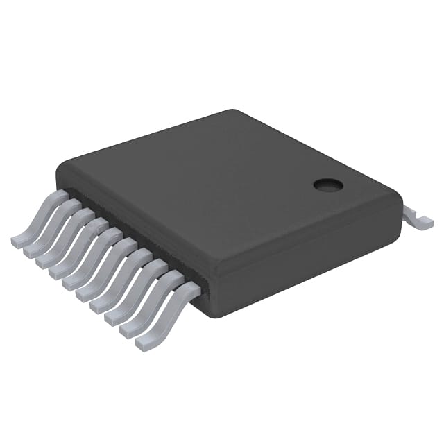
- Package: TSSOP (Thin Shrink Small Outline Package)
- Essence: High-speed, low-power buffer with 3-state outputs
- Packaging/Quantity: Tape and Reel, 2500 pieces per reel
Specifications
The SN74LVC244ADGVRG4 is an octal bus buffer that operates at a low voltage and utilizes CMOS logic. It is designed to provide high-speed buffering and line driving capabilities for various digital systems. The device features 3-state outputs, allowing multiple devices to be connected to a common bus without any conflicts.
Key specifications of the SN74LVC244ADGVRG4 include:
- Supply Voltage Range: 1.65V to 5.5V
- High-Speed Operation: 20 ns maximum propagation delay
- Low Power Consumption: ICC = 4µA maximum
- Output Drive Capability: ±24mA
- ESD Protection: Human Body Model > 2000V
Pin Configuration
The SN74LVC244ADGVRG4 has a total of 20 pins, which are arranged in a TSSOP package. The pin configuration is as follows:
Pin 1:  A1
   Pin 2:  Y1
   Pin 3:  A2
   Pin 4:  Y2
   Pin 5:  GND
   Pin 6:  Y3
   Pin 7:  A3
   Pin 8:  Y4
   Pin 9:  VCC
   Pin 10: Y5
   Pin 11: A4
   Pin 12: Y6
   Pin 13: A5
   Pin 14: Y7
   Pin 15: GND
   Pin 16: Y8
   Pin 17: OE#
   Pin 18: GND
   Pin 19: A6
   Pin 20: A7
Functional Features
The SN74LVC244ADGVRG4 offers the following functional features:
- Octal Buffer: Provides buffering for up to eight input lines.
- 3-State Outputs: Allows multiple devices to be connected to a common bus without any conflicts.
- Low Voltage Operation: Operates at a supply voltage as low as 1.65V, making it suitable for low-power applications.
- High-Speed Operation: Offers a maximum propagation delay of 20 ns, ensuring fast data transmission.
- ESD Protection: Incorporates ESD protection to safeguard against electrostatic discharge.
Advantages and Disadvantages
Advantages of the SN74LVC244ADGVRG4 include:
- Low power consumption
- High-speed operation
- 3-state outputs for bus sharing
- Wide supply voltage range
Disadvantages of the SN74LVC244ADGVRG4 include:
- Limited output drive capability
- TSSOP package may require careful handling during assembly
Working Principles
The SN74LVC244ADGVRG4 operates by receiving input signals on its eight input pins (A1-A7) and driving the corresponding output pins (Y1-Y8) based on the logic levels of the inputs. The OE# pin is used to enable or disable the outputs. When the OE# pin is high, the outputs are in the high-impedance state (disconnected from the bus), allowing other devices to drive the bus. When the OE# pin is low, the outputs are active and mirror the logic levels of the inputs.
Detailed Application Field Plans
The SN74LVC244ADGVRG4 is commonly used in various digital systems where buffering and line driving capabilities are required. Some specific application fields include:
- Microcontrollers: The buffer can be used to interface microcontrollers with other devices, such as memory chips or peripheral modules.
- Communication Systems: It can be employed in communication systems to amplify and drive signals between different components.
- Industrial Automation: The buffer finds applications in industrial automation systems for signal conditioning and level shifting purposes.
- Automotive Electronics: It can be utilized in automotive electronics for data bus buffering and signal isolation.
Detailed and Complete Alternative Models
Some alternative models that offer similar functionality to the SN74LVC244ADGVRG4 include:
- 74HC244: This is a popular alternative that operates at a higher voltage range (2V to 6V) but offers comparable performance.
- SN74LVCH244A: This model operates at a lower voltage range (1.65V to 3.6V) and provides improved ESD
Senaraikan 10 soalan dan jawapan biasa yang berkaitan dengan aplikasi SN74LVC244ADGVRG4 dalam penyelesaian teknikal
Sure! Here are 10 common questions and answers related to the application of SN74LVC244ADGVRG4:
Q: What is SN74LVC244ADGVRG4? A: SN74LVC244ADGVRG4 is a high-performance octal buffer and line driver with 3-state outputs, commonly used in digital systems.
Q: What is the operating voltage range for SN74LVC244ADGVRG4? A: The operating voltage range for SN74LVC244ADGVRG4 is typically between 1.65V and 5.5V.
Q: What is the maximum output current that SN74LVC244ADGVRG4 can drive? A: SN74LVC244ADGVRG4 can drive up to 32mA of output current per channel.
Q: Can SN74LVC244ADGVRG4 be used for level shifting applications? A: Yes, SN74LVC244ADGVRG4 can be used for level shifting as it supports both 3.3V and 5V logic levels.
Q: How many input/output channels does SN74LVC244ADGVRG4 have? A: SN74LVC244ADGVRG4 has 8 input/output channels.
Q: Does SN74LVC244ADGVRG4 have built-in protection features? A: Yes, SN74LVC244ADGVRG4 has built-in ESD (Electrostatic Discharge) protection on its inputs and outputs.
Q: What is the propagation delay of SN74LVC244ADGVRG4? A: The propagation delay of SN74LVC244ADGVRG4 is typically around 3.8ns.
Q: Can SN74LVC244ADGVRG4 be used in bidirectional applications? A: No, SN74LVC244ADGVRG4 is a unidirectional buffer and line driver, not suitable for bidirectional applications.
Q: What is the package type of SN74LVC244ADGVRG4? A: SN74LVC244ADGVRG4 is available in a small form factor TSSOP-20 package.
Q: Is SN74LVC244ADGVRG4 RoHS compliant? A: Yes, SN74LVC244ADGVRG4 is RoHS (Restriction of Hazardous Substances) compliant, making it environmentally friendly.
Please note that these answers are general and may vary depending on specific datasheet specifications and application requirements.