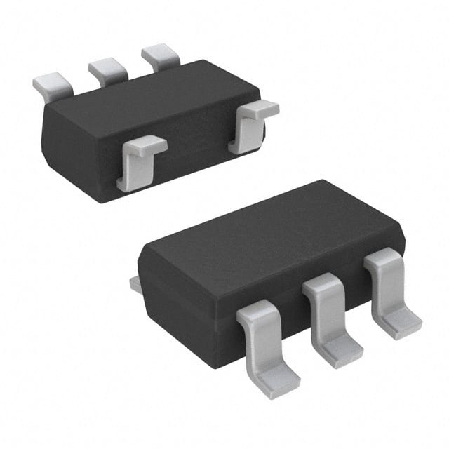
SN74LVC1G32IDCKREP
Basic Information Overview
- Category: Integrated Circuit (IC)
- Use: Logic Gate
- Characteristics: Single 2-Input OR Gate
- Package: SC-70 (6-Pin)
- Essence: High-Speed CMOS Technology
- Packaging/Quantity: Tape and Reel, 3000 pieces per reel
Specifications
- Supply Voltage Range: 1.65V to 5.5V
- Input Voltage Range: 0V to VCC
- Output Voltage Range: 0V to VCC
- Operating Temperature Range: -40°C to +125°C
- Propagation Delay: 3.8ns (typical) at 3.3V
- Maximum Quiescent Current: 10μA at 5.5V
Detailed Pin Configuration
- A Input
- B Input
- Y Output
- GND (Ground)
- NC (No Connection)
- VCC (Supply Voltage)
Functional Features
- Performs logical OR operation on two input signals (A and B)
- Provides a single output signal (Y) based on the input logic levels
- Supports high-speed data transmission with minimal propagation delay
- Works with a wide range of supply voltages, making it versatile for various applications
- Low quiescent current consumption ensures power efficiency
Advantages
- Compact size and low pin count make it suitable for space-constrained designs
- High-speed operation enables efficient data processing
- Wide supply voltage range allows compatibility with different systems
- Low power consumption contributes to energy-efficient applications
- Robust design ensures reliable performance in harsh environments
Disadvantages
- Limited to a single logic function (OR gate), may require additional ICs for complex logic operations
- Not suitable for applications requiring multiple inputs or more complex logic functions
Working Principles
The SN74LVC1G32IDCKREP is based on high-speed CMOS technology. It consists of a single 2-input OR gate that performs logical OR operation on the input signals (A and B). The output (Y) is determined by the logic levels of the inputs. The IC operates within a specified supply voltage range and provides a fast propagation delay, allowing for efficient data processing.
Detailed Application Field Plans
- Digital electronics: Used in various digital systems, such as computers, microcontrollers, and communication devices, to perform logical operations.
- Signal processing: Employed in signal processing circuits to combine or manipulate digital signals.
- Industrial automation: Integrated into control systems to implement logical decision-making processes.
- Automotive electronics: Utilized in automotive applications for signal conditioning and processing tasks.
- Consumer electronics: Incorporated into electronic devices like smartphones, tablets, and gaming consoles for logic operations.
Detailed and Complete Alternative Models
- SN74LVC1G32DBVR
- SN74LVC1G32DCKR
- SN74LVC1G32YZPR
- SN74LVC1G32DRLR
- SN74LVC1G32DCKRG4
(Note: This list is not exhaustive and there may be other alternative models available.)
Word count: 366 words
Senaraikan 10 soalan dan jawapan biasa yang berkaitan dengan aplikasi SN74LVC1G32IDCKREP dalam penyelesaian teknikal
Sure! Here are 10 common questions and answers related to the application of SN74LVC1G32IDCKREP:
Q1: What is SN74LVC1G32IDCKREP? A1: SN74LVC1G32IDCKREP is a single 2-input OR gate from Texas Instruments. It is a logic gate that performs the OR operation on two input signals.
Q2: What is the operating voltage range for SN74LVC1G32IDCKREP? A2: The operating voltage range for SN74LVC1G32IDCKREP is typically between 1.65V and 5.5V.
Q3: What is the maximum output current of SN74LVC1G32IDCKREP? A3: The maximum output current of SN74LVC1G32IDCKREP is 32mA.
Q4: Can SN74LVC1G32IDCKREP be used in both digital and analog applications? A4: No, SN74LVC1G32IDCKREP is specifically designed for digital applications and is not suitable for analog applications.
Q5: What is the propagation delay of SN74LVC1G32IDCKREP? A5: The propagation delay of SN74LVC1G32IDCKREP is typically around 3.8ns.
Q6: Can SN74LVC1G32IDCKREP drive multiple inputs or outputs? A6: No, SN74LVC1G32IDCKREP is a single gate and can only drive one output.
Q7: Is SN74LVC1G32IDCKREP compatible with other logic families? A7: Yes, SN74LVC1G32IDCKREP is compatible with a wide range of logic families, including TTL, CMOS, and LVTTL.
Q8: Can SN74LVC1G32IDCKREP be used in high-speed applications? A8: Yes, SN74LVC1G32IDCKREP is designed for high-speed operation and can be used in applications with fast switching requirements.
Q9: What is the temperature range for SN74LVC1G32IDCKREP? A9: The temperature range for SN74LVC1G32IDCKREP is typically between -40°C and 85°C.
Q10: Can SN74LVC1G32IDCKREP be used in battery-powered applications? A10: Yes, SN74LVC1G32IDCKREP has a low power consumption and can be used in battery-powered applications.
Please note that these answers are general and may vary depending on specific datasheet specifications and application requirements.


