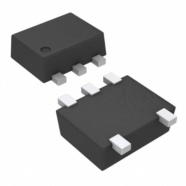
SN74LVC1G04DRLRG4
Product Overview
- Category: Integrated Circuit (IC)
- Use: Logic Gate
- Characteristics: Single Inverter Gate
- Package: SOT-553
- Essence: High-Speed CMOS Technology
- Packaging/Quantity: Tape and Reel, 3000 pieces per reel
Specifications
- Supply Voltage Range: 1.65V to 5.5V
- Input Voltage Range: 0V to VCC
- Output Voltage Range: 0V to VCC
- Maximum Operating Frequency: 100 MHz
- Propagation Delay: 3.8 ns (typical)
- Input Capacitance: 2 pF (typical)
- Output Drive Capability: ±24 mA
Detailed Pin Configuration
The SN74LVC1G04DRLRG4 has a total of 5 pins:
- GND (Ground): Connected to the ground reference of the circuit.
- VCC (Supply Voltage): Connected to the positive supply voltage.
- A (Input): Input pin for the logic gate.
- Y (Output): Output pin for the logic gate.
- NC (No Connection): This pin is not connected and should be left unconnected.
Functional Features
- Single Inverter Gate: The SN74LVC1G04DRLRG4 is a single inverter gate that performs the logical inversion of the input signal.
- High-Speed CMOS Technology: It utilizes high-speed CMOS technology, allowing for fast switching times and low power consumption.
- Wide Supply Voltage Range: The IC can operate within a wide supply voltage range, making it compatible with various systems.
- Small Package Size: The SOT-553 package is compact, enabling space-saving designs in applications with limited board space.
Advantages and Disadvantages
Advantages: - High-speed operation - Low power consumption - Wide supply voltage range - Small package size
Disadvantages: - Limited functionality (only performs logical inversion)
Working Principles
The SN74LVC1G04DRLRG4 operates based on the principles of CMOS logic. When a logic high (VCC) is applied to the input pin (A), the output pin (Y) will be at logic low (GND). Conversely, when a logic low (GND) is applied to the input pin (A), the output pin (Y) will be at logic high (VCC). This logical inversion is achieved through the internal circuitry of the IC.
Detailed Application Field Plans
The SN74LVC1G04DRLRG4 can be used in various applications, including but not limited to:
- Digital Systems: It can be used as a building block for digital systems, such as microcontrollers, FPGAs, and ASICs.
- Signal Conditioning: The logic inversion capability makes it suitable for signal conditioning applications, where the polarity of the input signal needs to be inverted.
- Level Shifting: It can be used for level shifting between different voltage domains in mixed-signal systems.
- Clock Generation: The inverter gate can be utilized in clock generation circuits to generate complementary clock signals.
Detailed and Complete Alternative Models
- SN74LVC1G04DBVR: SOT-23 package, 3000 pieces per reel
- SN74LVC1G04DCKR: SC-70 package, 3000 pieces per reel
- SN74LVC1G04YZPR: DSBGA package, 3000 pieces per reel
- SN74LVC1G04QDCKRQ1: Automotive-grade, SC-70 package, 3000 pieces per reel
These alternative models offer similar functionality and characteristics to the SN74LVC1G04DRLRG4, providing options for different package preferences or specific application requirements.
Word count: 431 words
Senaraikan 10 soalan dan jawapan biasa yang berkaitan dengan aplikasi SN74LVC1G04DRLRG4 dalam penyelesaian teknikal
Sure! Here are 10 common questions and answers related to the application of SN74LVC1G04DRLRG4 in technical solutions:
Q1: What is SN74LVC1G04DRLRG4? A1: SN74LVC1G04DRLRG4 is a single inverter gate IC (Integrated Circuit) that is commonly used in digital logic circuits.
Q2: What is the voltage supply range for SN74LVC1G04DRLRG4? A2: The voltage supply range for SN74LVC1G04DRLRG4 is typically between 1.65V and 5.5V.
Q3: What is the maximum output current of SN74LVC1G04DRLRG4? A3: The maximum output current of SN74LVC1G04DRLRG4 is typically around 32mA.
Q4: Can SN74LVC1G04DRLRG4 be used as a level shifter? A4: Yes, SN74LVC1G04DRLRG4 can be used as a level shifter to convert signals from one voltage level to another.
Q5: What is the propagation delay of SN74LVC1G04DRLRG4? A5: The propagation delay of SN74LVC1G04DRLRG4 is typically around 4.3ns.
Q6: Can SN74LVC1G04DRLRG4 be used in high-speed applications? A6: Yes, SN74LVC1G04DRLRG4 is suitable for high-speed applications due to its low propagation delay and fast switching characteristics.
Q7: Is SN74LVC1G04DRLRG4 compatible with both CMOS and TTL logic levels? A7: Yes, SN74LVC1G04DRLRG4 is compatible with both CMOS (Complementary Metal-Oxide-Semiconductor) and TTL (Transistor-Transistor Logic) logic levels.
Q8: Can SN74LVC1G04DRLRG4 be used in battery-powered applications? A8: Yes, SN74LVC1G04DRLRG4 can be used in battery-powered applications as it operates at low voltage levels and has low power consumption.
Q9: What is the package type of SN74LVC1G04DRLRG4? A9: SN74LVC1G04DRLRG4 is available in a small SOT-23-5 package.
Q10: Can SN74LVC1G04DRLRG4 be used in automotive applications? A10: Yes, SN74LVC1G04DRLRG4 is suitable for automotive applications as it meets the necessary standards and specifications for automotive electronics.
Please note that the answers provided here are general and may vary depending on specific datasheet and application requirements.


