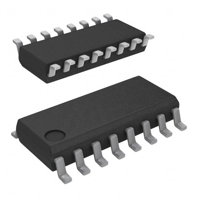
SN74LVC157AD
Product Overview
Category
SN74LVC157AD belongs to the category of integrated circuits (ICs).
Use
This IC is commonly used in digital electronics for data multiplexing applications.
Characteristics
- Low-voltage CMOS technology
- 2-input multiplexer with four binary inputs
- Wide operating voltage range: 1.65V to 5.5V
- High-speed operation: 5.4 ns propagation delay at 3.3V
- Low power consumption: 10µA maximum ICC
- Schmitt-trigger inputs for noise immunity
- Available in various package options
Package and Quantity
SN74LVC157AD is available in a small-outline integrated circuit (SOIC) package. It is typically sold in reels or tubes containing multiple units.
Specifications
- Supply Voltage Range: 1.65V to 5.5V
- Input Voltage Range: 0V to VCC
- Output Voltage Range: 0V to VCC
- Operating Temperature Range: -40°C to +85°C
- Maximum Propagation Delay: 5.4 ns at 3.3V
- Maximum Power Dissipation: 500mW
Pin Configuration
The SN74LVC157AD IC has a total of 16 pins, which are assigned specific functions as follows:
Pin 1: A0
Pin 2: B0
Pin 3: Y0
Pin 4: A1
Pin 5: B1
Pin 6: Y1
Pin 7: GND
Pin 8: Y2
Pin 9: B2
Pin 10: A2
Pin 11: Y3
Pin 12: B3
Pin 13: A3
Pin 14: VCC
Pin 15: G1
Pin 16: G2
Functional Features
The SN74LVC157AD is a 2-input multiplexer with four binary inputs. It allows the selection of one of the four input signals based on the control inputs. The Schmitt-trigger inputs provide noise immunity, making it suitable for applications in noisy environments.
Advantages and Disadvantages
Advantages
- Wide operating voltage range allows compatibility with various systems
- Low power consumption makes it energy-efficient
- High-speed operation enables quick data processing
- Schmitt-trigger inputs ensure reliable performance in noisy conditions
Disadvantages
- Limited number of input channels (four)
- May not be suitable for applications requiring more complex multiplexing functionality
Working Principles
The SN74LVC157AD operates by selecting one of the four input signals based on the control inputs. The selected input is then routed to the output pin. The IC utilizes low-voltage CMOS technology, which ensures efficient power usage and high-speed operation.
Application Field Plans
The SN74LVC157AD finds applications in various fields, including: 1. Data communication systems 2. Digital signal processing 3. Industrial automation 4. Consumer electronics 5. Automotive electronics
Alternative Models
Here are some alternative models that can be used as substitutes for SN74LVC157AD: 1. CD74HC157E 2. MC74VHC157DT 3. 74LVC157APW
These alternative models offer similar functionality and characteristics, providing flexibility in design choices.
In conclusion, the SN74LVC157AD is a versatile integrated circuit used for data multiplexing applications. Its low-voltage CMOS technology, wide operating voltage range, and high-speed operation make it suitable for various digital electronics projects. However, its limited number of input channels may restrict its use in more complex multiplexing scenarios.
Senaraikan 10 soalan dan jawapan biasa yang berkaitan dengan aplikasi SN74LVC157AD dalam penyelesaian teknikal
Sure! Here are 10 common questions and answers related to the application of SN74LVC157AD:
Q: What is SN74LVC157AD? A: SN74LVC157AD is a quad 2-input multiplexer IC (Integrated Circuit) that can be used in various technical solutions.
Q: What is the purpose of SN74LVC157AD? A: SN74LVC157AD is used to select one of four data inputs and route it to a single output based on the control inputs.
Q: What is the voltage range supported by SN74LVC157AD? A: SN74LVC157AD supports a wide voltage range from 1.65V to 5.5V, making it compatible with different systems.
Q: How many control inputs does SN74LVC157AD have? A: SN74LVC157AD has two control inputs, which determine the selection of the data input.
Q: Can SN74LVC157AD handle high-speed signals? A: Yes, SN74LVC157AD is designed for high-speed operation and can handle signals up to several hundred megahertz.
Q: What is the maximum current rating of SN74LVC157AD? A: The maximum current rating for each output of SN74LVC157AD is typically around 24mA.
Q: Can SN74LVC157AD be cascaded to increase the number of inputs? A: Yes, multiple SN74LVC157AD ICs can be cascaded together to increase the number of inputs and outputs.
Q: Is SN74LVC157AD suitable for battery-powered applications? A: Yes, SN74LVC157AD is designed to operate at low power and is suitable for battery-powered applications.
Q: What is the package type of SN74LVC157AD? A: SN74LVC157AD is available in various package types, such as SOIC (Small Outline Integrated Circuit) and TSSOP (Thin Shrink Small Outline Package).
Q: Are there any application notes or reference designs available for SN74LVC157AD? A: Yes, Texas Instruments provides application notes and reference designs that can help in implementing SN74LVC157AD in different technical solutions.
Please note that these answers are general and may vary depending on specific datasheets and manufacturer guidelines.


