

SN74LVC04ADGVRE4
Basic Information Overview
- Category: Integrated Circuit (IC)
- Use: Logic Gate
- Characteristics:
- Low-voltage CMOS technology
- High-speed operation
- Wide operating voltage range
- Low power consumption
- Package: VSON (Very Small Outline No-Lead) package
- Essence: Hex Inverter
- Packaging/Quantity: Tape and Reel, 2500 units per reel
Specifications
- Supply Voltage Range: 1.65V to 5.5V
- Input Voltage Range: 0V to VCC
- Output Voltage Range: 0V to VCC
- Operating Temperature Range: -40°C to +85°C
- Propagation Delay Time: 3.8ns (typical)
- Maximum Quiescent Current: 10μA
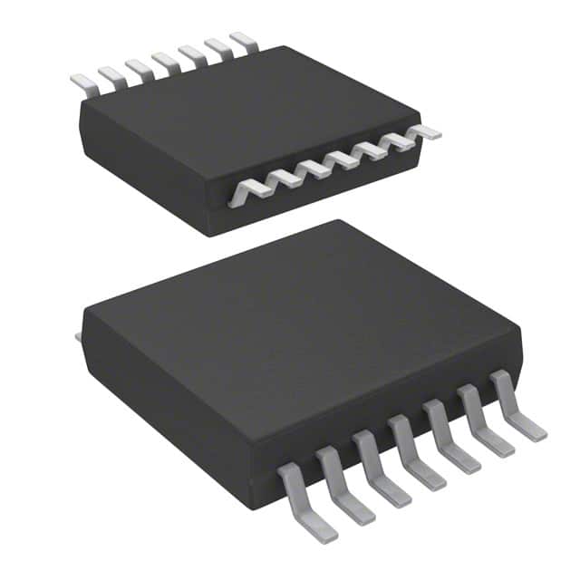
Detailed Pin Configuration
The SN74LVC04ADGVRE4 has a total of 14 pins, numbered as follows:
- A1 (Input)
- Y1 (Output)
- A2 (Input)
- Y2 (Output)
- A3 (Input)
- Y3 (Output)
- GND (Ground)
- Y4 (Output)
- A4 (Input)
- Y5 (Output)
- A5 (Input)
- Y6 (Output)
- VCC (Power Supply)
- GND (Ground)
Functional Features
- Hex inverter with six independent inverters
- Compatible with TTL and CMOS logic levels
- Provides high noise immunity
- Allows direct interface with different logic families
- Supports bidirectional level translation
Advantages and Disadvantages
Advantages: - Low-voltage operation allows for compatibility with various systems - High-speed operation enables efficient signal processing - Wide operating voltage range provides flexibility in different applications - Low power consumption reduces energy requirements
Disadvantages: - Limited number of inverters (six) in a single package - May not be suitable for applications requiring a large number of logic gates
Working Principles
The SN74LVC04ADGVRE4 is a hex inverter IC that performs the logical NOT operation on its input signals. It utilizes low-voltage CMOS technology, which allows it to operate at lower power supply voltages while maintaining high-speed performance. The IC consists of six independent inverters, each capable of converting a logic high input to a logic low output and vice versa.
Detailed Application Field Plans
The SN74LVC04ADGVRE4 finds application in various digital systems where logic inversion is required. Some common application fields include: - Microcontrollers and microprocessors - Data communication systems - Industrial automation - Consumer electronics - Automotive electronics
Detailed and Complete Alternative Models
- SN74LVC04APW - TSSOP (Thin Shrink Small Outline Package), 14 pins
- SN74LVC04ADR - SOIC (Small Outline Integrated Circuit), 14 pins
- SN74LVC04ANSR - SOT23-5 (Small Outline Transistor), 5 pins
- SN74LVC04ARGYR - VQFN (Very Thin Quad Flat No-Lead), 16 pins
These alternative models offer similar functionality and characteristics to the SN74LVC04ADGVRE4, but may differ in package type and pin configuration.
Word count: 315 words
Senaraikan 10 soalan dan jawapan biasa yang berkaitan dengan aplikasi SN74LVC04ADGVRE4 dalam penyelesaian teknikal
Sure! Here are 10 common questions and answers related to the application of SN74LVC04ADGVRE4 in technical solutions:
Q: What is SN74LVC04ADGVRE4? A: SN74LVC04ADGVRE4 is a hex inverter IC (integrated circuit) that consists of six independent inverters.
Q: What is the voltage supply range for SN74LVC04ADGVRE4? A: The voltage supply range for SN74LVC04ADGVRE4 is typically between 1.65V and 5.5V.
Q: What is the maximum output current of SN74LVC04ADGVRE4? A: The maximum output current of SN74LVC04ADGVRE4 is typically 32mA.
Q: Can SN74LVC04ADGVRE4 be used with both CMOS and TTL logic levels? A: Yes, SN74LVC04ADGVRE4 is compatible with both CMOS and TTL logic levels.
Q: What is the operating temperature range for SN74LVC04ADGVRE4? A: The operating temperature range for SN74LVC04ADGVRE4 is typically between -40°C and 85°C.
Q: How many pins does SN74LVC04ADGVRE4 have? A: SN74LVC04ADGVRE4 is available in a 14-pin TSSOP (Thin Shrink Small Outline Package).
Q: Can SN74LVC04ADGVRE4 be used in high-speed applications? A: Yes, SN74LVC04ADGVRE4 is designed for high-speed operation and can be used in various high-frequency applications.
Q: What is the power dissipation of SN74LVC04ADGVRE4? A: The power dissipation of SN74LVC04ADGVRE4 is typically 0.8mW per gate.
Q: Can SN74LVC04ADGVRE4 be used in battery-powered applications? A: Yes, SN74LVC04ADGVRE4 has a low power consumption and can be used in battery-powered applications.
Q: What are some typical applications of SN74LVC04ADGVRE4? A: SN74LVC04ADGVRE4 can be used in various applications such as signal inversion, level shifting, line driving, and interfacing between different logic families.
Please note that the answers provided here are general and may vary depending on specific datasheet specifications and application requirements.