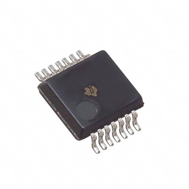
SN74LVC00ADBRG4
Product Overview
- Category: Integrated Circuit (IC)
- Use: Logic Gate
- Characteristics: Quad 2-Input NAND Gate
- Package: SSOP-14
- Essence: High-speed CMOS technology
- Packaging/Quantity: Tape and Reel, 2500 pieces per reel
Specifications
- Supply Voltage Range: 1.65V to 5.5V
- Input Voltage Range: 0V to VCC
- Output Voltage Range: 0V to VCC
- Maximum Operating Frequency: 200MHz
- Propagation Delay Time: 3.8ns (typical)
- Low Power Consumption: ICC = 2μA (maximum)
Detailed Pin Configuration
The SN74LVC00ADBRG4 has a total of 14 pins arranged as follows:
__    __
   Y1 |1  \/  14| VCC
   A1 |2       13| B1
   A2 |3       12| B2
   Y2 |4       11| C1
  GND |5       10| C2
   A3 |6        9| D1
   B3 |7        8| D2
       --    --
Functional Features
- Quad 2-input NAND gate with Schmitt-trigger inputs
- Compatible with TTL levels
- High-speed operation
- Low power consumption
- Wide supply voltage range
- Overvoltage tolerant inputs
- Balanced propagation delays
- ESD protection exceeds JESD 22
Advantages and Disadvantages
Advantages: - High-speed operation allows for efficient data processing. - Low power consumption reduces energy usage. - Wide supply voltage range provides flexibility in various applications. - Overvoltage tolerant inputs protect the IC from voltage spikes. - Balanced propagation delays ensure accurate timing.
Disadvantages: - Limited to quad 2-input NAND gate functionality. - May not be suitable for applications requiring more complex logic functions.
Working Principles
The SN74LVC00ADBRG4 is a quad 2-input NAND gate that utilizes high-speed CMOS technology. It operates by accepting two input signals and producing an inverted output signal. The Schmitt-trigger inputs allow for noise immunity and hysteresis, ensuring reliable operation even in noisy environments. The IC is designed to operate within a wide supply voltage range, making it compatible with various systems.
Detailed Application Field Plans
The SN74LVC00ADBRG4 can be used in a wide range of applications, including but not limited to:
- Digital logic circuits
- Microcontrollers and microprocessors
- Communication systems
- Industrial automation
- Automotive electronics
- Consumer electronics
Its compatibility with TTL levels and low power consumption make it suitable for battery-powered devices and energy-efficient systems. The high-speed operation enables efficient data processing in time-critical applications.
Detailed and Complete Alternative Models
- SN74LVC00APWR - TSSOP-14 package
- SN74LVC00ANSR - SOP-14 package
- SN74LVC00ADGVR - TVSOP-14 package
- SN74LVC00ADGVRE4 - TVSOP-14 package (reel)
These alternative models offer similar functionality and characteristics to the SN74LVC00ADBRG4, providing options for different packaging requirements or preferences.
In conclusion, the SN74LVC00ADBRG4 is a quad 2-input NAND gate IC that offers high-speed operation, low power consumption, and wide supply voltage range. Its versatile applications, compatibility with TTL levels, and balanced propagation delays make it a reliable choice for various digital logic circuits.
Senaraikan 10 soalan dan jawapan biasa yang berkaitan dengan aplikasi SN74LVC00ADBRG4 dalam penyelesaian teknikal
Sure! Here are 10 common questions and answers related to the application of SN74LVC00ADBRG4 in technical solutions:
Q: What is SN74LVC00ADBRG4? A: SN74LVC00ADBRG4 is a quad 2-input NAND gate integrated circuit (IC) that is commonly used in digital logic applications.
Q: What is the operating voltage range of SN74LVC00ADBRG4? A: The operating voltage range of SN74LVC00ADBRG4 is from 1.65V to 5.5V.
Q: What is the maximum output current of SN74LVC00ADBRG4? A: The maximum output current of SN74LVC00ADBRG4 is typically 32mA.
Q: Can SN74LVC00ADBRG4 be used in both CMOS and TTL logic systems? A: Yes, SN74LVC00ADBRG4 is compatible with both CMOS and TTL logic systems.
Q: What is the propagation delay of SN74LVC00ADBRG4? A: The propagation delay of SN74LVC00ADBRG4 is typically around 4.3ns.
Q: Can SN74LVC00ADBRG4 be used in high-speed applications? A: Yes, SN74LVC00ADBRG4 is designed for high-speed operation and can be used in various high-frequency applications.
Q: Does SN74LVC00ADBRG4 have built-in protection against electrostatic discharge (ESD)? A: Yes, SN74LVC00ADBRG4 has built-in ESD protection to ensure reliable operation in ESD-prone environments.
Q: Can SN74LVC00ADBRG4 drive capacitive loads? A: Yes, SN74LVC00ADBRG4 can drive capacitive loads up to a certain limit specified in the datasheet.
Q: Is SN74LVC00ADBRG4 available in different package options? A: Yes, SN74LVC00ADBRG4 is available in various package options, such as SOIC, TSSOP, and VQFN.
Q: What are some typical applications of SN74LVC00ADBRG4? A: SN74LVC00ADBRG4 can be used in a wide range of applications, including digital logic circuits, signal conditioning, level shifting, and interface design.
Please note that the answers provided here are general and may vary depending on specific datasheet specifications and application requirements.


