

SN74LV08ADGVR
Product Overview
- Category: Integrated Circuit (IC)
- Use: Logic Gate
- Characteristics: Quad 2-input AND gate
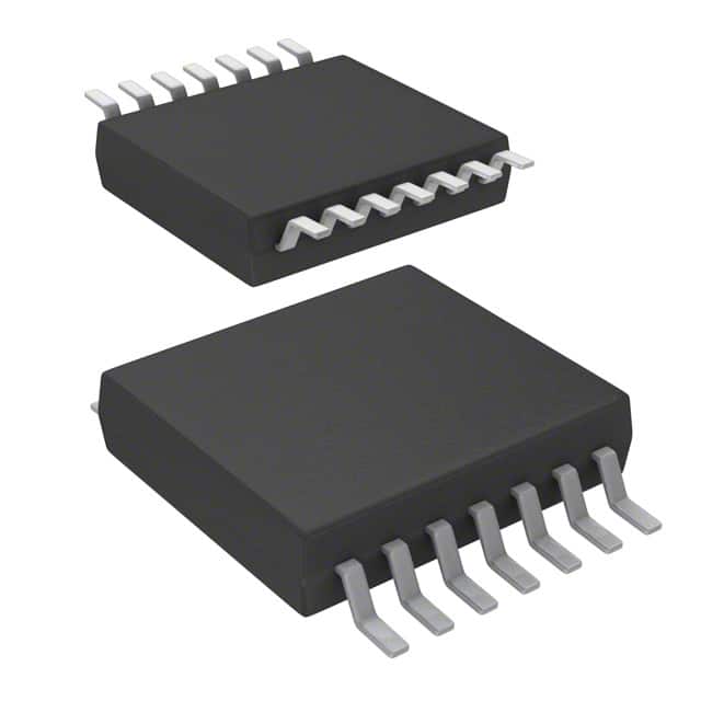
- Package: VSSOP (Very Small Outline Package)
- Essence: High-performance CMOS technology
- Packaging/Quantity: Tape and Reel, 2500 units per reel
Specifications
- Supply Voltage Range: 1.65V to 5.5V
- Input Voltage Range: 0V to VCC
- Output Voltage Range: 0V to VCC
- Operating Temperature Range: -40°C to +85°C
- Propagation Delay Time: 4.3ns (typical)
- Maximum Quiescent Current: 10μA
- Maximum Output Current: ±8mA
Detailed Pin Configuration
The SN74LV08ADGVR has a total of 14 pins, which are arranged as follows:
__    __
   Y1 |1  \__/ 14| VCC
   A1 |2        13| B1
   B2 |3        12| A2
   Y2 |4   SN   11| GND
  GND |5   74   10| Y3
   A3 |6   LV   9 | C1
   C2 |7   08   8 | Y4
       --        --
Functional Features
- Quad 2-input AND gate: The SN74LV08ADGVR consists of four independent AND gates, each with two inputs and one output.
- High-speed operation: Utilizing high-performance CMOS technology, this IC provides fast propagation delay times, making it suitable for applications requiring quick response.
- Wide voltage range: The supply voltage range of 1.65V to 5.5V allows compatibility with various power sources.
- Low power consumption: With a maximum quiescent current of only 10μA, the SN74LV08ADGVR is energy-efficient.
Advantages and Disadvantages
Advantages: - High-speed operation - Wide voltage range - Low power consumption - Compact VSSOP package
Disadvantages: - Limited number of inputs (2 per gate) - Not suitable for high-current applications
Working Principles
The SN74LV08ADGVR operates based on the principles of Boolean logic. Each of the four AND gates within the IC compares the logical states of its two input signals and produces an output signal that is the logical AND of the inputs. The internal circuitry utilizes CMOS technology to achieve fast switching speeds and low power consumption.
Detailed Application Field Plans
The SN74LV08ADGVR finds application in various digital systems where logical AND operations are required. Some common application fields include:
- Digital signal processing
- Microcontrollers and microprocessors
- Communication systems
- Industrial automation
- Consumer electronics
Detailed and Complete Alternative Models
- SN74LV08ADR: SOIC (Small Outline Integrated Circuit) package variant
- SN74LV08APWR: TSSOP (Thin Shrink Small Outline Package) package variant
- SN74LV08ARGYR: QFN (Quad Flat No-leads) package variant
These alternative models offer similar functionality but differ in package type, making them suitable for different PCB layouts and assembly processes.
Word count: 305 words
Senaraikan 10 soalan dan jawapan biasa yang berkaitan dengan aplikasi SN74LV08ADGVR dalam penyelesaian teknikal
Sure! Here are 10 common questions and answers related to the application of SN74LV08ADGVR:
Q: What is SN74LV08ADGVR? A: SN74LV08ADGVR is a quad 2-input AND gate IC (integrated circuit) from Texas Instruments.
Q: What is the voltage supply range for SN74LV08ADGVR? A: The voltage supply range for SN74LV08ADGVR is typically between 1.65V and 5.5V.
Q: What is the maximum operating frequency of SN74LV08ADGVR? A: The maximum operating frequency of SN74LV08ADGVR is typically around 125 MHz.
Q: Can SN74LV08ADGVR be used in both digital and analog circuits? A: No, SN74LV08ADGVR is specifically designed for digital logic applications.
Q: How many AND gates are there in SN74LV08ADGVR? A: SN74LV08ADGVR contains four independent AND gates.
Q: What is the output current capability of SN74LV08ADGVR? A: The output current capability of SN74LV08ADGVR is typically around 8 mA.
Q: Is SN74LV08ADGVR compatible with TTL (Transistor-Transistor Logic) inputs? A: Yes, SN74LV08ADGVR is fully compatible with TTL inputs.
Q: Can SN74LV08ADGVR tolerate overvoltage on its inputs? A: No, SN74LV08ADGVR is not designed to tolerate overvoltage on its inputs. It is recommended to stay within the specified voltage range.
Q: What is the package type for SN74LV08ADGVR? A: SN74LV08ADGVR comes in a small-sized VSSOP (Very Small Outline Package) with 8 pins.
Q: Can SN74LV08ADGVR be used in automotive applications? A: Yes, SN74LV08ADGVR is suitable for use in automotive applications as it meets the necessary standards and requirements.
Please note that these answers are general and may vary depending on the specific datasheet and application requirements.