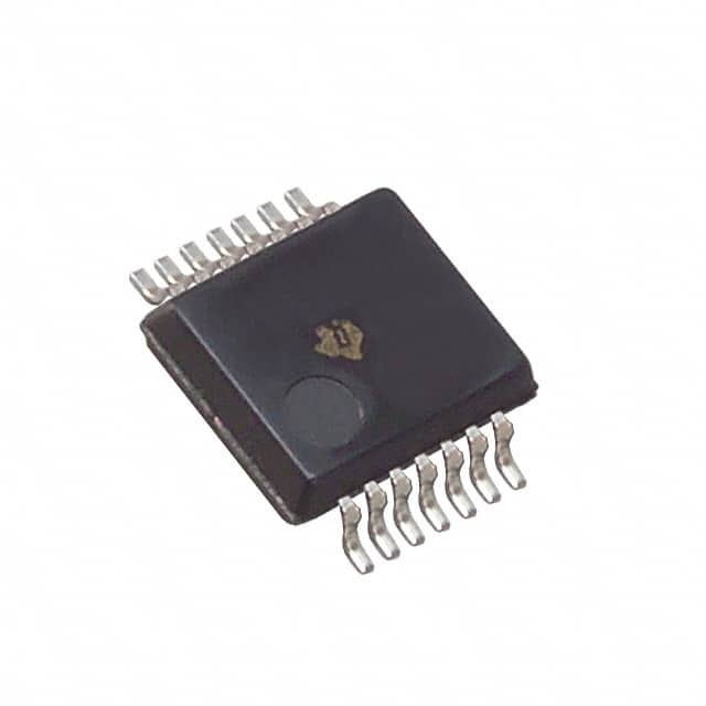
SN74HC05DBRG4
Product Overview
- Category: Integrated Circuit
- Use: Logic Gate
- Characteristics: Hex Inverter with Open-Drain Outputs
- Package: 14-Pin TSSOP (Thin Shrink Small Outline Package)
- Essence: High-Speed CMOS Logic
- Packaging/Quantity: Tape and Reel, 2500 units per reel
Specifications
- Supply Voltage Range: 2V to 6V
- Input Voltage Range: 0V to VCC
- Output Voltage Range: 0V to VCC
- Maximum Operating Frequency: 50 MHz
- Propagation Delay Time: 10 ns (typical)
- Operating Temperature Range: -40°C to +85°C
Detailed Pin Configuration
The SN74HC05DBRG4 has a total of 14 pins. The pin configuration is as follows:
- A1 - Input 1 for Inverter 1
- Y1 - Output for Inverter 1
- A2 - Input 2 for Inverter 2
- Y2 - Output for Inverter 2
- A3 - Input 3 for Inverter 3
- Y3 - Output for Inverter 3
- GND - Ground
- Y4 - Output for Inverter 4
- A4 - Input 4 for Inverter 4
- Y5 - Output for Inverter 5
- A5 - Input 5 for Inverter 5
- Y6 - Output for Inverter 6
- A6 - Input 6 for Inverter 6
- VCC - Power Supply
Functional Features
- Hex inverter with open-drain outputs
- High-speed operation
- Wide supply voltage range
- Compatible with TTL and CMOS logic levels
- Low power consumption
- Schmitt-trigger input for noise immunity
Advantages and Disadvantages
Advantages: - Open-drain outputs allow easy interfacing with other devices - High-speed operation enables quick signal processing - Wide supply voltage range provides flexibility in different applications - Compatibility with TTL and CMOS logic levels ensures versatility - Low power consumption reduces energy usage - Schmitt-trigger input enhances noise immunity, improving signal integrity
Disadvantages: - Limited number of inverters (6) compared to larger ICs - Not suitable for high-frequency applications above 50 MHz
Working Principles
The SN74HC05DBRG4 is a hex inverter with open-drain outputs. It operates by taking the input signal and producing the inverted output signal. The open-drain outputs allow the device to be connected to other devices or components without conflicts in voltage levels.
The IC uses high-speed CMOS logic, which enables fast switching times and efficient signal processing. It has a wide supply voltage range of 2V to 6V, making it compatible with various power sources. The Schmitt-trigger input provides noise immunity, ensuring reliable operation even in noisy environments.
Detailed Application Field Plans
The SN74HC05DBRG4 can be used in various applications, including but not limited to:
- Digital communication systems
- Microcontrollers and microprocessors
- Industrial automation
- Automotive electronics
- Consumer electronics
- Power management systems
- Robotics and control systems
Detailed and Complete Alternative Models
- SN74HC04DBRG4 - Hex Inverter
- SN74HCT05DBRG4 - Hex Inverter with Schmitt-Trigger Inputs
- SN74LVC06ADBR - Hex Inverter Buffer/Driver with Open-Drain Outputs
- SN74LV1T04DBVR - Single Inverter with Open-Drain Output
These alternative models offer similar functionality and can be used as substitutes for the SN74HC05DBRG4 in various applications.
In conclusion, the SN74HC05DBRG4 is a hex inverter IC with open-drain outputs. It offers high-speed operation, wide supply voltage range, and compatibility with TTL and CMOS logic levels. Its functional features, advantages, and application versatility make it a suitable choice for a wide range of digital and analog circuits.
Senaraikan 10 soalan dan jawapan biasa yang berkaitan dengan aplikasi SN74HC05DBRG4 dalam penyelesaian teknikal
Sure! Here are 10 common questions and answers related to the application of SN74HC05DBRG4 in technical solutions:
Q: What is SN74HC05DBRG4? A: SN74HC05DBRG4 is a hex inverter with open-drain outputs, which means it can invert input signals and drive them to an open-drain output.
Q: What is the voltage supply range for SN74HC05DBRG4? A: The voltage supply range for SN74HC05DBRG4 is typically between 2V and 6V.
Q: What is the maximum output current that SN74HC05DBRG4 can sink? A: SN74HC05DBRG4 can sink a maximum output current of 25mA.
Q: Can SN74HC05DBRG4 be used as a level shifter? A: Yes, SN74HC05DBRG4 can be used as a level shifter to convert signals between different voltage levels.
Q: How many inputs and outputs does SN74HC05DBRG4 have? A: SN74HC05DBRG4 has six inputs and six open-drain outputs.
Q: What is the propagation delay of SN74HC05DBRG4? A: The propagation delay of SN74HC05DBRG4 is typically around 9ns.
Q: Can SN74HC05DBRG4 be used in high-speed applications? A: Yes, SN74HC05DBRG4 can be used in high-speed applications as it has a fast propagation delay.
Q: Is SN74HC05DBRG4 compatible with both CMOS and TTL logic levels? A: Yes, SN74HC05DBRG4 is compatible with both CMOS and TTL logic levels.
Q: Can SN74HC05DBRG4 be used in automotive applications? A: Yes, SN74HC05DBRG4 is suitable for automotive applications as it has a wide voltage supply range and can operate in harsh environments.
Q: What is the package type of SN74HC05DBRG4? A: SN74HC05DBRG4 comes in a small-outline integrated circuit (SOIC) package.
Please note that these answers are general and may vary depending on specific application requirements and datasheet specifications.


