

SN74AUP2G08RSER
Product Overview
- Category: Integrated Circuit
- Use: Logic Gate
- Characteristics: Dual 2-input AND gate
- Package: Small Outline Package (SOP)
- Essence: High-performance, low-power consumption logic gate
- Packaging/Quantity: Tape and Reel, 3000 units per reel
Specifications
- Supply Voltage Range: 0.8V to 3.6V
- Input Voltage Range: -0.5V to VCC + 0.5V
- Output Voltage Range: 0V to VCC
- Operating Temperature Range: -40°C to 85°C
- Propagation Delay: 1.9ns (typical)
- Maximum Quiescent Current: 10μA
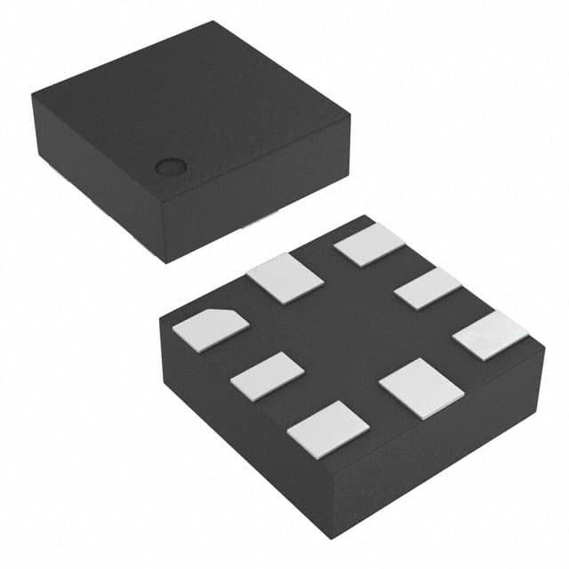
Detailed Pin Configuration
The SN74AUP2G08RSER has a total of 6 pins:
- Pin 1: Input A
- Pin 2: Input B
- Pin 3: Ground (GND)
- Pin 4: Output Y
- Pin 5: Power Supply (VCC)
- Pin 6: No Connection (NC)
Functional Features
- Dual 2-input AND gate with Schmitt-trigger inputs
- Low power consumption
- High-speed operation
- Wide operating voltage range
- ESD protection on all inputs and outputs
- Compatible with TTL and CMOS logic levels
Advantages and Disadvantages
Advantages: - Low power consumption makes it suitable for battery-powered devices - High-speed operation allows for efficient data processing - Wide operating voltage range provides flexibility in various applications - ESD protection ensures reliability and durability
Disadvantages: - Limited number of inputs (only two) - Not suitable for complex logic operations requiring multiple inputs
Working Principles
The SN74AUP2G08RSER is a dual 2-input AND gate that performs logical AND operations on two input signals (A and B). It utilizes Schmitt-trigger inputs, which provide hysteresis and improve noise immunity. The gate operates within a wide voltage range, making it compatible with various logic levels. When both inputs are high, the output Y becomes high; otherwise, it remains low.
Detailed Application Field Plans
The SN74AUP2G08RSER is commonly used in the following applications:
- Battery-powered devices: Due to its low power consumption, it is suitable for use in portable electronics such as smartphones, tablets, and wearables.
- Industrial automation: The gate's high-speed operation makes it ideal for controlling and processing signals in industrial control systems.
- Automotive electronics: With its wide operating voltage range and ESD protection, it is well-suited for automotive applications, including engine control units, infotainment systems, and sensor interfaces.
Detailed and Complete Alternative Models
- SN74AUP2G08DCTR: Similar to SN74AUP2G08RSER but available in a different package (SOT-23)
- SN74LVC2G08DCUR: Dual 2-input AND gate with similar characteristics but operates at higher voltages (1.65V to 5.5V)
- SN74HC08N: Quad 2-input AND gate with similar functionality but offers four inputs instead of two
(Note: This list is not exhaustive and other alternative models may exist.)
Word count: 346 words
Senaraikan 10 soalan dan jawapan biasa yang berkaitan dengan aplikasi SN74AUP2G08RSER dalam penyelesaian teknikal
Sure! Here are 10 common questions and answers related to the application of SN74AUP2G08RSER in technical solutions:
Q: What is SN74AUP2G08RSER? A: SN74AUP2G08RSER is a dual 2-input positive-AND gate IC (integrated circuit) manufactured by Texas Instruments.
Q: What is the voltage supply range for SN74AUP2G08RSER? A: The voltage supply range for SN74AUP2G08RSER is typically between 0.8V and 3.6V.
Q: What is the maximum output current of SN74AUP2G08RSER? A: The maximum output current of SN74AUP2G08RSER is 32mA.
Q: Can SN74AUP2G08RSER be used in battery-powered applications? A: Yes, SN74AUP2G08RSER can be used in battery-powered applications due to its low power consumption and wide voltage supply range.
Q: What is the operating temperature range for SN74AUP2G08RSER? A: The operating temperature range for SN74AUP2G08RSER is typically between -40°C and 85°C.
Q: How many gates are there in SN74AUP2G08RSER? A: SN74AUP2G08RSER has two independent AND gates.
Q: What is the propagation delay of SN74AUP2G08RSER? A: The propagation delay of SN74AUP2G08RSER is typically around 2.5ns.
Q: Can SN74AUP2G08RSER be used in high-speed applications? A: Yes, SN74AUP2G08RSER can be used in high-speed applications due to its low propagation delay and fast switching characteristics.
Q: Is SN74AUP2G08RSER compatible with other logic families? A: Yes, SN74AUP2G08RSER is compatible with a wide range of logic families, including CMOS, TTL, and LVTTL.
Q: What are some typical applications of SN74AUP2G08RSER? A: Some typical applications of SN74AUP2G08RSER include signal conditioning, level shifting, data routing, and general-purpose digital logic design.
Please note that the answers provided here are general and may vary depending on specific datasheet specifications and application requirements.