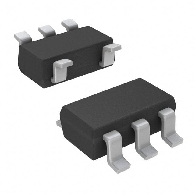
SN74AUP1G34DCKTG4
Product Overview
- Category: Integrated Circuit
- Use: Logic Gate
- Characteristics: Single Buffer/Driver, Non-Inverting, Open Drain Output
- Package: SC-70 (6-Pin)
- Essence: This integrated circuit is a single buffer/driver with a non-inverting open drain output. It is designed to be used in various digital logic applications.
- Packaging/Quantity: The SN74AUP1G34DCKTG4 is available in tape and reel packaging, with 3000 units per reel.
Specifications
- Supply Voltage Range: 0.8V to 3.6V
- Input Voltage Range: 0V to VCC
- Output Voltage Range: 0V to VCC
- Operating Temperature Range: -40°C to +85°C
- Propagation Delay Time: 2.5ns (typical)
- Output Current: ±4mA
Detailed Pin Configuration
The SN74AUP1G34DCKTG4 has the following pin configuration:
- GND (Ground)
- A (Input)
- Y (Output)
- NC (No Connection)
- VCC (Power Supply)
- B (Input)
Functional Features
- Single buffer/driver with non-inverting open drain output
- High-speed operation with low power consumption
- Wide supply voltage range allows compatibility with various systems
- Schmitt-trigger input for improved noise immunity
- ESD protection on all pins for enhanced reliability
Advantages
- Small package size enables space-saving designs
- Low power consumption extends battery life in portable devices
- High-speed operation improves overall system performance
- Wide supply voltage range provides flexibility in different applications
- ESD protection ensures robustness against electrostatic discharge
Disadvantages
- Limited output current may not be suitable for high-current applications
- Open drain output requires external pull-up resistor for proper operation
Working Principles
The SN74AUP1G34DCKTG4 operates as a buffer/driver with a non-inverting open drain output. It receives an input signal and amplifies it to drive the output pin. The open drain output allows the device to be connected to other devices or circuits, requiring an external pull-up resistor to provide the desired logic level.
Detailed Application Field Plans
The SN74AUP1G34DCKTG4 can be used in various digital logic applications, including but not limited to:
- Communication systems
- Data transmission
- Industrial automation
- Consumer electronics
- Automotive electronics
- Medical devices
- Internet of Things (IoT) devices
Detailed and Complete Alternative Models
Some alternative models that can be considered as alternatives to the SN74AUP1G34DCKTG4 are:
- SN74LVC1G34DBVR
- SN74LV1T34DBVR
- SN74AHC1G34DBVR
- SN74AHCT1G34DBVR
- SN74LVC1G34DCKR
These models offer similar functionality and characteristics, providing options for different design requirements.
In conclusion, the SN74AUP1G34DCKTG4 is a single buffer/driver integrated circuit with a non-inverting open drain output. It offers high-speed operation, low power consumption, and wide supply voltage range. While it has limitations in terms of output current and the need for an external pull-up resistor, it finds applications in various fields such as communication systems, data transmission, and consumer electronics. Alternative models are available to cater to different design needs.
Senaraikan 10 soalan dan jawapan biasa yang berkaitan dengan aplikasi SN74AUP1G34DCKTG4 dalam penyelesaian teknikal
Sure! Here are 10 common questions and answers related to the application of SN74AUP1G34DCKTG4 in technical solutions:
Q1: What is SN74AUP1G34DCKTG4? A1: SN74AUP1G34DCKTG4 is a single buffer gate IC (Integrated Circuit) that operates at a voltage range of 0.8V to 3.6V. It is commonly used for level shifting, signal buffering, and voltage translation applications.
Q2: What is the maximum output current of SN74AUP1G34DCKTG4? A2: The maximum output current of SN74AUP1G34DCKTG4 is typically around 32mA.
Q3: Can SN74AUP1G34DCKTG4 be used for bidirectional level shifting? A3: No, SN74AUP1G34DCKTG4 is a unidirectional buffer gate and cannot be used for bidirectional level shifting. For bidirectional level shifting, you would need a different type of IC.
Q4: What is the propagation delay of SN74AUP1G34DCKTG4? A4: The propagation delay of SN74AUP1G34DCKTG4 is typically around 1.5ns.
Q5: Can SN74AUP1G34DCKTG4 handle 5V signals? A5: No, SN74AUP1G34DCKTG4 is not designed to handle 5V signals. Its voltage range is limited to 0.8V to 3.6V.
Q6: Is SN74AUP1G34DCKTG4 suitable for high-speed applications? A6: Yes, SN74AUP1G34DCKTG4 is designed for high-speed applications and can operate at frequencies up to several hundred megahertz.
Q7: Can SN74AUP1G34DCKTG4 be used as a level shifter between different voltage domains? A7: Yes, SN74AUP1G34DCKTG4 can be used as a level shifter between different voltage domains, as long as the voltage levels are within its specified range of 0.8V to 3.6V.
Q8: What is the package type of SN74AUP1G34DCKTG4? A8: SN74AUP1G34DCKTG4 is available in a small SOT-23-5 package.
Q9: Does SN74AUP1G34DCKTG4 have any built-in protection features? A9: No, SN74AUP1G34DCKTG4 does not have any built-in protection features. It is important to ensure that the input and output voltages stay within the specified range to prevent damage.
Q10: Can SN74AUP1G34DCKTG4 be used in battery-powered applications? A10: Yes, SN74AUP1G34DCKTG4 can be used in battery-powered applications as it operates at low voltage levels and has low power consumption.
Please note that these answers are general and may vary depending on specific application requirements and datasheet specifications.


