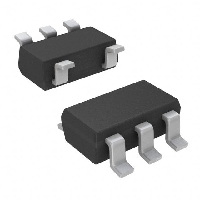
SN74AUC1G08DCKR
Product Overview
- Category: Integrated Circuit
- Use: Logic Gate
- Characteristics: Single 2-Input AND Gate
- Package: SC-70 (6-Pin)
- Essence: High-Speed CMOS Technology
- Packaging/Quantity: Tape and Reel, 3000 pieces per reel
Specifications
- Supply Voltage Range: 0.8V to 3.6V
- High-Speed Operation: tpd = 2.5ns (typ) at 3.3V
- Low Power Consumption: ICC = 0.9µA (max) at TA = 25°C
- Schmitt-Trigger Inputs for Noise Immunity
- ESD Protection Exceeds JESD 22
Detailed Pin Configuration
The SN74AUC1G08DCKR has a 6-pin SC-70 package with the following pin configuration:
```
| | --|1 2|-- --|3 4|-- --|5 6|-- |____| ```
Pin 1: Input A Pin 2: Ground Pin 3: Output Y Pin 4: VCC Pin 5: Input B Pin 6: Not Connected
Functional Features
- Single 2-Input AND Gate
- High-Speed operation for quick signal processing
- Low power consumption for energy efficiency
- Schmitt-Trigger inputs provide noise immunity
- ESD protection ensures device durability
Advantages and Disadvantages
Advantages: - High-speed operation allows for fast data processing - Low power consumption reduces energy usage - Schmitt-Trigger inputs provide noise immunity, ensuring reliable performance - ESD protection enhances device durability
Disadvantages: - Limited to 2-input AND gate functionality - Not suitable for applications requiring more complex logic operations
Working Principles
The SN74AUC1G08DCKR is a single 2-input AND gate that operates using high-speed CMOS technology. It takes two input signals, A and B, and produces an output signal, Y, based on the logical AND operation of the inputs. The gate utilizes Schmitt-Trigger inputs to provide noise immunity, ensuring reliable operation even in noisy environments. The device operates within a supply voltage range of 0.8V to 3.6V and consumes low power, making it suitable for various battery-powered applications.
Detailed Application Field Plans
The SN74AUC1G08DCKR can be used in a wide range of applications that require logical AND operations. Some potential application fields include:
- Digital Logic Design: The gate can be used as a building block in digital circuits to implement various logical functions.
- Microcontrollers and Processors: It can be utilized in microcontroller and processor designs to perform logical operations on input signals.
- Communication Systems: The gate can be employed in communication systems to process and control data flow.
- Industrial Automation: It can be integrated into industrial automation systems for controlling and monitoring processes.
- Consumer Electronics: The gate finds applications in consumer electronics devices such as smartphones, tablets, and gaming consoles.
Detailed and Complete Alternative Models
Some alternative models to SN74AUC1G08DCKR that serve similar functions include:
- SN74AHC1G08DBVR: Single 2-Input AND Gate with AHC Technology
- SN74LVC1G08DCKR: Single 2-Input AND Gate with LVC Technology
- SN74LV1T08DBVR: Single 2-Input AND Gate with LV Technology
- SN74HC08DCKR: Quad 2-Input AND Gate with HC Technology
These alternative models provide similar functionality but may differ in terms of speed, power consumption, voltage range, and package type.
In conclusion, the SN74AUC1G08DCKR is a single 2-input AND gate integrated circuit that operates using high-speed CMOS technology. It offers advantages such as high-speed operation, low power consumption, noise immunity, and ESD protection. The gate finds applications in various fields including digital logic design, microcontrollers, communication systems, industrial automation, and consumer electronics. Alternative models with similar functionality are also available in the market.
Senaraikan 10 soalan dan jawapan biasa yang berkaitan dengan aplikasi SN74AUC1G08DCKR dalam penyelesaian teknikal
Sure! Here are 10 common questions and answers related to the application of SN74AUC1G08DCKR:
Q1: What is SN74AUC1G08DCKR? A1: SN74AUC1G08DCKR is a single 2-input AND gate IC (integrated circuit) manufactured by Texas Instruments.
Q2: What is the operating voltage range of SN74AUC1G08DCKR? A2: The operating voltage range of SN74AUC1G08DCKR is from 0.8V to 3.6V.
Q3: What is the maximum output current of SN74AUC1G08DCKR? A3: The maximum output current of SN74AUC1G08DCKR is 32mA.
Q4: Can SN74AUC1G08DCKR be used in battery-powered applications? A4: Yes, SN74AUC1G08DCKR can be used in battery-powered applications due to its low power consumption and wide operating voltage range.
Q5: What is the package type of SN74AUC1G08DCKR? A5: SN74AUC1G08DCKR comes in a small SOT-353 package.
Q6: What is the typical propagation delay of SN74AUC1G08DCKR? A6: The typical propagation delay of SN74AUC1G08DCKR is around 2.7ns.
Q7: Can SN74AUC1G08DCKR be used in high-speed applications? A7: Yes, SN74AUC1G08DCKR is suitable for high-speed applications due to its fast switching speed and low propagation delay.
Q8: Is SN74AUC1G08DCKR compatible with other logic families? A8: Yes, SN74AUC1G08DCKR is compatible with a wide range of logic families, including TTL, CMOS, and LVTTL.
Q9: Can SN74AUC1G08DCKR be used in automotive applications? A9: Yes, SN74AUC1G08DCKR is automotive-grade and can be used in various automotive applications.
Q10: What are some typical applications of SN74AUC1G08DCKR? A10: Some typical applications of SN74AUC1G08DCKR include signal conditioning, level shifting, clock distribution, and general-purpose logic functions.
Please note that these answers are general and may vary depending on specific design requirements.


