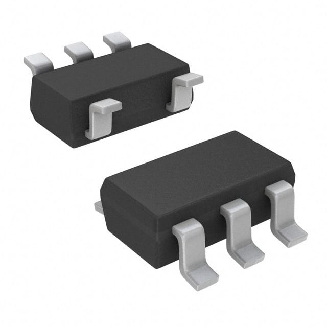
SN74AUC1G07DCKTG4
Product Overview
Category
SN74AUC1G07DCKTG4 belongs to the category of integrated circuits (ICs).
Use
This IC is commonly used as a buffer/driver in various electronic devices and systems.
Characteristics
- Low power consumption
- High-speed operation
- Wide operating voltage range
- Small package size
- RoHS compliant
Package
SN74AUC1G07DCKTG4 is available in a small SOT-23-5 package.
Essence
The essence of SN74AUC1G07DCKTG4 lies in its ability to provide buffering and driving capabilities for digital signals, ensuring reliable signal transmission within electronic circuits.
Packaging/Quantity
SN74AUC1G07DCKTG4 is typically packaged in reels, with each reel containing 3000 units of the IC.
Specifications
- Supply Voltage Range: 0.8V to 3.6V
- Input Voltage Range: 0V to VCC
- Output Voltage Range: 0V to VCC
- Maximum Operating Frequency: 500 MHz
- Number of Pins: 5
- Operating Temperature Range: -40°C to +85°C
Detailed Pin Configuration
SN74AUC1G07DCKTG4 has the following pin configuration:
____
   A1 |    | VCC
   A2 |    | Y
 GND  |____| A
Functional Features
- Buffering: SN74AUC1G07DCKTG4 acts as a buffer, amplifying weak input signals to ensure proper signal levels at the output.
- Driving: It can drive capacitive loads, enabling efficient signal transmission across long traces or cables.
- High-Speed Operation: The IC operates at high speeds, making it suitable for applications requiring fast signal propagation.
Advantages and Disadvantages
Advantages
- Low power consumption makes it ideal for battery-powered devices.
- Wide operating voltage range allows compatibility with various systems.
- Small package size saves board space in compact designs.
- RoHS compliance ensures environmental friendliness.
Disadvantages
- Limited number of pins may restrict its use in complex circuits.
- High-frequency operation may introduce signal integrity issues in certain applications.
Working Principles
SN74AUC1G07DCKTG4 works by receiving digital input signals on pin A and amplifying them to a higher voltage level. The amplified signals are then available at the output pin Y. The IC operates based on complementary metal-oxide-semiconductor (CMOS) technology, which enables low power consumption and high-speed operation.
Detailed Application Field Plans
SN74AUC1G07DCKTG4 finds applications in various fields, including:
- Consumer Electronics: Used in smartphones, tablets, and portable media players for signal buffering and driving.
- Automotive: Employed in automotive electronics for signal conditioning and level shifting.
- Industrial Automation: Utilized in control systems and PLCs for reliable signal transmission.
- Telecommunications: Integrated into networking equipment for signal amplification and line driving.
- Medical Devices: Incorporated in medical instruments for signal processing and amplification.
Detailed and Complete Alternative Models
Some alternative models that can be considered as alternatives to SN74AUC1G07DCKTG4 include:
- SN74LVC1G07DBVR
- SN74HC1G07DCKR
- SN74LV1T34DBVR
- SN74AUP1G07DCKR
- SN74LVC1G07DCKR
These models offer similar functionality and characteristics, providing flexibility in choosing the most suitable IC for specific applications.
Word count: 536
Senaraikan 10 soalan dan jawapan biasa yang berkaitan dengan aplikasi SN74AUC1G07DCKTG4 dalam penyelesaian teknikal
Sure! Here are 10 common questions and answers related to the application of SN74AUC1G07DCKTG4 in technical solutions:
1. What is SN74AUC1G07DCKTG4? - SN74AUC1G07DCKTG4 is a single buffer/driver with open-drain output, designed for use in various digital logic applications.
2. What is the operating voltage range of SN74AUC1G07DCKTG4? - The operating voltage range of SN74AUC1G07DCKTG4 is from 0.8V to 3.6V.
3. What is the maximum output current of SN74AUC1G07DCKTG4? - The maximum output current of SN74AUC1G07DCKTG4 is typically 32mA.
4. Can SN74AUC1G07DCKTG4 be used as a level shifter? - Yes, SN74AUC1G07DCKTG4 can be used as a level shifter to convert signals between different voltage levels.
5. What is the typical propagation delay of SN74AUC1G07DCKTG4? - The typical propagation delay of SN74AUC1G07DCKTG4 is around 2.7ns.
6. Is SN74AUC1G07DCKTG4 suitable for high-speed applications? - Yes, SN74AUC1G07DCKTG4 is designed for high-speed operation and can be used in applications requiring fast switching times.
7. Can SN74AUC1G07DCKTG4 drive capacitive loads? - Yes, SN74AUC1G07DCKTG4 can drive small capacitive loads typically found in digital logic circuits.
8. Does SN74AUC1G07DCKTG4 have built-in protection features? - Yes, SN74AUC1G07DCKTG4 has built-in ESD (electrostatic discharge) protection to safeguard against static electricity damage.
9. Can SN74AUC1G07DCKTG4 be used in battery-powered applications? - Yes, SN74AUC1G07DCKTG4's low operating voltage range makes it suitable for battery-powered applications with limited power supply.
10. Is SN74AUC1G07DCKTG4 available in different package options? - Yes, SN74AUC1G07DCKTG4 is available in various package options, including SOT-23 and SC-70, providing flexibility for different design requirements.
Please note that the answers provided here are general and may vary depending on the specific application and conditions. It is always recommended to refer to the datasheet and consult the manufacturer for detailed information and guidelines.


