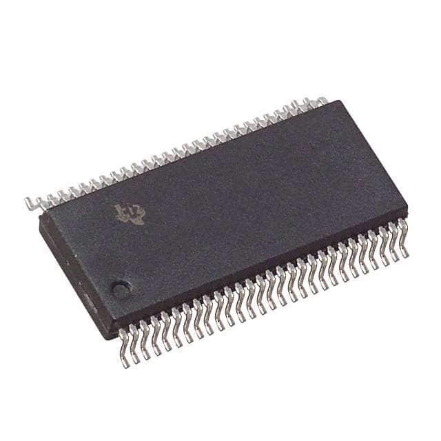
SN74ALVTH162827LR
Product Overview
- Category: Integrated Circuit (IC)
- Use: Logic Level Translator
- Characteristics:
- High-speed operation
- Low power consumption
- Wide voltage range
- Bidirectional translation capability
- Package: 56-pin TSSOP (Thin Shrink Small Outline Package)
- Essence: Logic level translation between different voltage domains
- Packaging/Quantity: Tape and Reel, 2500 units per reel
Specifications
- Supply Voltage Range: 1.2V to 3.6V
- Input Voltage Range: 0V to VCC
- Output Voltage Range: 0V to VCC
- Operating Temperature Range: -40°C to +85°C
- Propagation Delay: 2.5ns (typical)
- Output Drive Strength: ±24mA
Detailed Pin Configuration
The SN74ALVTH162827LR has a total of 56 pins. The pin configuration is as follows:
- OE1B
- A1
- B1
- Y1
- GND
- Y2
- B2
- A2
- OE2B
- VCC
- OE1A
- A1
- B1
- Y1
- GND
- Y2
- B2
- A2
- OE2A
- VCC
- Y3
- B3
- A3
- OE3B
- GND
- OE4B
- A4
- B4
- Y4
- VCC
- OE3A
- A3
- B3
- Y3
- GND
- OE4A
- B4
- A4
- OE5B
- VCC
- Y5
- B5
- A5
- OE5A
- GND
- OE6B
- A6
- B6
- Y6
- VCC
- OE6A
- B6
- A6
- OE7B
- GND
- Y7
Functional Features
- Bidirectional voltage level translation between two voltage domains
- Automatic direction sensing and control
- High-speed operation allows for efficient data transfer
- Low power consumption for energy-efficient applications
- Wide voltage range compatibility for versatile usage scenarios
Advantages and Disadvantages
Advantages: - High-speed operation enables fast data transmission - Low power consumption prolongs battery life in portable devices - Wide voltage range compatibility makes it suitable for various applications - Bidirectional translation simplifies circuit design
Disadvantages: - Limited number of translation channels (7 in this case) - Requires careful consideration of voltage levels to avoid signal distortion
Working Principles
The SN74ALVTH162827LR is designed to translate logic levels between two different voltage domains. It features bidirectional translation, allowing data to flow in both directions. The device automatically senses the direction of data flow and adjusts the voltage levels accordingly.
The IC operates by using a combination of voltage level shifters and control circuitry. When a high-level signal is applied to the input pin of one voltage domain, the corresponding output pin in the other voltage domain will also produce a high-level signal, and vice versa.
Detailed Application Field Plans
The SN74ALVTH162827LR can be used in various applications that require logic level translation between different voltage domains. Some potential application fields include:
- Microcontroller interfacing with different voltage peripherals
- Communication systems involving multiple voltage levels
- Battery-powered devices requiring efficient level shifting
- Industrial automation and control systems
- Automotive electronics
Detailed and Complete Alternative Models
- SN74ALVTH162827DLR: Similar specifications and features, but available in a smaller package (48-pin TSSOP).
- SN74LVC4245APWR: Octal bus transceiver with similar voltage range and bidirectional capability.
- SN74AVC4T245RGYR: Quad-bit level shifter with 3-state outputs and wide voltage range compatibility.
These alternative models offer similar functionality and can be considered as substitutes for the SN74ALVTH162827LR depending on specific requirements and constraints.
Word count: 524 words
Senaraikan 10 soalan dan jawapan biasa yang berkaitan dengan aplikasi SN74ALVTH162827LR dalam penyelesaian teknikal
Sure! Here are 10 common questions and answers related to the application of SN74ALVTH162827LR:
Q: What is SN74ALVTH162827LR? A: SN74ALVTH162827LR is a 20-bit universal bus driver with 3-state outputs, designed for low-voltage (1.65V to 3.6V) applications.
Q: What is the maximum operating frequency of SN74ALVTH162827LR? A: The maximum operating frequency of SN74ALVTH162827LR is typically around 400 MHz.
Q: Can SN74ALVTH162827LR be used in both input and output applications? A: Yes, SN74ALVTH162827LR can be used as both an input buffer and an output driver.
Q: What is the purpose of the 3-state outputs in SN74ALVTH162827LR? A: The 3-state outputs allow multiple devices to share a common bus without interfering with each other.
Q: What is the voltage level compatibility of SN74ALVTH162827LR? A: SN74ALVTH162827LR is compatible with both TTL and CMOS voltage levels.
Q: Can SN74ALVTH162827LR handle bidirectional data flow? A: No, SN74ALVTH162827LR is a unidirectional device and can only drive data in one direction.
Q: What is the typical output current capability of SN74ALVTH162827LR? A: The typical output current capability of SN74ALVTH162827LR is around 12 mA.
Q: Does SN74ALVTH162827LR have built-in ESD protection? A: Yes, SN74ALVTH162827LR has built-in ESD protection to safeguard against electrostatic discharge.
Q: Can SN74ALVTH162827LR be used in automotive applications? A: Yes, SN74ALVTH162827LR is suitable for automotive applications as it meets the necessary standards and requirements.
Q: What is the package type of SN74ALVTH162827LR? A: SN74ALVTH162827LR is available in a 56-pin TSSOP (Thin Shrink Small Outline Package) package.
Please note that these answers are general and may vary depending on specific datasheet specifications and application requirements.


