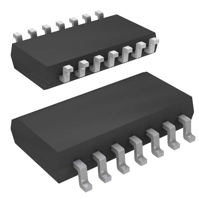
SN74ALS74ANSR
Product Overview
- Category: Integrated Circuit (IC)
- Use: Flip-Flop
- Characteristics: Dual D-Type Positive-Edge-Triggered Flip-Flop with Clear and Preset
- Package: SOIC (Small Outline Integrated Circuit)
- Essence: The SN74ALS74ANSR is a versatile flip-flop IC that can store and manipulate digital data. It is widely used in various electronic devices and systems.
- Packaging/Quantity: Available in tape and reel packaging, with 2500 units per reel.
Specifications
- Supply Voltage: 4.5V to 5.5V
- Logic Family: ALS (Advanced Low-Power Schottky)
- Number of Flip-Flops: 2
- Trigger Type: Positive Edge
- Clear and Preset Inputs: Yes
- Operating Temperature Range: -40°C to 85°C
- Propagation Delay: 9 ns (typical)
Detailed Pin Configuration
The SN74ALS74ANSR has a total of 14 pins, which are assigned specific functions as follows:
- CLR (Clear) - Active-Low Clear Input
- D1 (Data Input 1) - Data Input for Flip-Flop 1
- CP1 (Clock Pulse 1) - Clock Input for Flip-Flop 1
- PR1 (Preset 1) - Active-Low Preset Input for Flip-Flop 1
- Q1 (Output 1) - Output of Flip-Flop 1
- Q̅1 (Complementary Output 1) - Complementary Output of Flip-Flop 1
- GND (Ground) - Ground Reference
- Q̅2 (Complementary Output 2) - Complementary Output of Flip-Flop 2
- Q2 (Output 2) - Output of Flip-Flop 2
- PR2 (Preset 2) - Active-Low Preset Input for Flip-Flop 2
- CP2 (Clock Pulse 2) - Clock Input for Flip-Flop 2
- D2 (Data Input 2) - Data Input for Flip-Flop 2
- VCC (Supply Voltage) - Positive Power Supply
- CLR̅ (Complementary Clear) - Complementary Clear Input
Functional Features
- Dual flip-flop design allows independent storage and manipulation of two separate data inputs.
- Positive-edge triggering ensures reliable and synchronized data capture.
- Clear and preset inputs provide control over the initial state of the flip-flops.
- Complementary outputs facilitate versatile logic operations and signal routing.
Advantages and Disadvantages
Advantages: - Versatile functionality suitable for a wide range of applications. - Low power consumption due to the ALS logic family. - Compact SOIC package enables space-efficient circuit designs. - Reliable performance across a wide temperature range.
Disadvantages: - Limited number of flip-flops per IC (only two in this case). - Lack of asynchronous set or reset inputs may limit certain application scenarios. - Not compatible with higher voltage supply ranges.
Working Principles
The SN74ALS74ANSR operates based on the principles of positive-edge-triggered flip-flops. When a rising edge is detected at the clock input (CP1 or CP2), the data present at the corresponding data input (D1 or D2) is captured and stored in the respective flip-flop. The clear and preset inputs allow for initialization of the flip-flop states, while the complementary outputs provide inverted versions of the stored data. This IC operates within a specified voltage range and exhibits a propagation delay of approximately 9 ns.
Detailed Application Field Plans
The SN74ALS74ANSR finds applications in various digital systems, including but not limited to:
- Sequential logic circuits
- Data storage and retrieval systems
- Counters and frequency dividers
- State machines and control units
- Communication devices and protocols
- Microcontrollers and microprocessors
- Digital signal processing (DSP) systems
- Memory address decoding circuits
Detailed and Complete Alternative Models
- SN74LS74AN: Similar dual flip-flop IC with slightly different characteristics.
- CD4013BE: Dual D-Type Flip-Flop IC from another manufacturer.
- MC74HC74AN: High-Speed CMOS Dual D Flip-Flop IC.
- 74HCT74: Dual D-Type Flip-Flop IC compatible with higher voltage ranges.
These alternative models offer similar functionality and can be used as substitutes for the SN74ALS74ANSR depending on specific requirements and availability.
Word count: 529 words
Senaraikan 10 soalan dan jawapan biasa yang berkaitan dengan aplikasi SN74ALS74ANSR dalam penyelesaian teknikal
Sure! Here are 10 common questions and answers related to the application of SN74ALS74ANSR in technical solutions:
Q: What is SN74ALS74ANSR? A: SN74ALS74ANSR is a dual positive-edge-triggered D-type flip-flop integrated circuit (IC) that can store one bit of data.
Q: What are the key features of SN74ALS74ANSR? A: Some key features of SN74ALS74ANSR include low power consumption, high-speed operation, wide operating voltage range, and compatibility with TTL logic levels.
Q: How can SN74ALS74ANSR be used in technical solutions? A: SN74ALS74ANSR can be used for various applications such as data storage, synchronization, frequency division, and digital signal processing.
Q: What is the operating voltage range of SN74ALS74ANSR? A: The operating voltage range of SN74ALS74ANSR is typically between 4.5V and 5.5V.
Q: Can SN74ALS74ANSR work with both CMOS and TTL logic levels? A: Yes, SN74ALS74ANSR is compatible with both CMOS and TTL logic levels, making it versatile for different system designs.
Q: What is the maximum clock frequency supported by SN74ALS74ANSR? A: SN74ALS74ANSR can support clock frequencies up to several hundred megahertz, depending on the specific conditions and setup.
Q: Does SN74ALS74ANSR have any built-in protection features? A: Yes, SN74ALS74ANSR has built-in diode clamps on the inputs to protect against electrostatic discharge (ESD) events.
Q: Can SN74ALS74ANSR be used in both synchronous and asynchronous applications? A: Yes, SN74ALS74ANSR can be used in both synchronous and asynchronous applications, depending on the specific requirements of the system.
Q: What is the typical power consumption of SN74ALS74ANSR? A: The typical power consumption of SN74ALS74ANSR is relatively low, making it suitable for battery-powered or energy-efficient designs.
Q: Are there any recommended external components to use with SN74ALS74ANSR? A: It is generally recommended to use decoupling capacitors near the power supply pins of SN74ALS74ANSR to ensure stable operation and reduce noise.
Please note that these answers are general and may vary depending on the specific application and design considerations.


