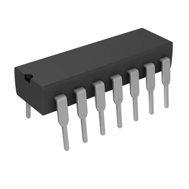
SN74ALS08NG4
Product Overview
- Category: Integrated Circuit (IC)
- Use: Logic Gate
- Characteristics: Quad 2-input AND gate
- Package: DIP-14 (Dual In-line Package with 14 pins)
- Essence: High-speed, low-power consumption logic gate
- Packaging/Quantity: Tube packaging, 25 pieces per tube
Specifications
- Supply Voltage Range: 4.5V to 5.5V
- Input Voltage Range: 0V to VCC
- Output Voltage Range: 0V to VCC
- Operating Temperature Range: -40°C to +85°C
- Propagation Delay Time: 9ns (typical)
- Power Dissipation: 22mW (typical)
Detailed Pin Configuration
The SN74ALS08NG4 has a total of 14 pins arranged as follows:
__    __
   Y1 --| 1    14 |-- VCC
   A1 --| 2    13 |-- B1
   B2 --| 3    12 |-- A2
   Y2 --| 4    11 |-- C1
   A2 --| 5    10 |-- B3
   B3 --| 6     9 |-- A3
   Y3 --| 7     8 |-- GND
        ----------
Functional Features
- Quad 2-input AND gate: The SN74ALS08NG4 consists of four independent AND gates, each with two inputs and one output.
- High-speed operation: The gate provides fast propagation delay time, making it suitable for applications requiring quick response times.
- Low-power consumption: The IC is designed to minimize power dissipation, making it energy-efficient.
- Wide operating temperature range: The SN74ALS08NG4 can operate reliably in a wide temperature range, from -40°C to +85°C.
Advantages and Disadvantages
Advantages: - High-speed operation allows for quick processing of logic signals. - Low-power consumption reduces energy usage and heat generation. - Wide operating temperature range ensures reliability in various environments.
Disadvantages: - Limited functionality: The SN74ALS08NG4 is specifically designed as a quad 2-input AND gate and may not be suitable for more complex logic operations. - DIP package: The dual in-line package may not be suitable for space-constrained applications.
Working Principles
The SN74ALS08NG4 operates based on the principles of digital logic. It performs the logical AND operation on two input signals and produces an output signal based on the following truth table:
| A | B | Y |
|---|---|---|
| 0 | 0 | 0 |
| 0 | 1 | 0 |
| 1 | 0 | 0 |
| 1 | 1 | 1 |
The gate uses transistors and other electronic components to implement this logical operation.
Detailed Application Field Plans
The SN74ALS08NG4 is commonly used in various digital systems and applications, including:
- Microprocessor-based systems
- Data communication equipment
- Industrial control systems
- Automotive electronics
- Consumer electronics
Its primary function as a logic gate makes it suitable for tasks such as signal conditioning, data routing, and logical decision-making within these applications.
Detailed and Complete Alternative Models
There are several alternative models available that offer similar functionality to the SN74ALS08NG4. Some popular alternatives include:
- 74HC08: This CMOS-based quad 2-input AND gate offers similar performance with lower power consumption.
- CD4081: This CMOS-based quad 2-input AND gate provides improved noise immunity and wider supply voltage range.
- SN54LS08: This TTL-based quad 2-input AND gate offers compatibility with older logic families.
These alternatives can be considered based on specific requirements, such as power consumption, voltage range, or compatibility with existing systems.
In conclusion, the SN74ALS08NG4 is a quad 2-input AND gate integrated circuit that offers high-speed operation, low-power consumption, and wide temperature range. It finds applications in various digital systems and has alternative models available for specific needs.
Senaraikan 10 soalan dan jawapan biasa yang berkaitan dengan aplikasi SN74ALS08NG4 dalam penyelesaian teknikal
Sure! Here are 10 common questions and answers related to the application of SN74ALS08NG4 in technical solutions:
Q: What is SN74ALS08NG4? A: SN74ALS08NG4 is a quad 2-input positive-AND gate integrated circuit (IC) that is commonly used in digital logic applications.
Q: What is the operating voltage range for SN74ALS08NG4? A: The operating voltage range for SN74ALS08NG4 is typically between 4.5V and 5.5V.
Q: What is the maximum input current for SN74ALS08NG4? A: The maximum input current for SN74ALS08NG4 is 0.1mA.
Q: Can SN74ALS08NG4 be used in high-speed applications? A: Yes, SN74ALS08NG4 is designed for high-speed operation and can be used in such applications.
Q: What is the output drive capability of SN74ALS08NG4? A: SN74ALS08NG4 has a typical output drive capability of 8mA.
Q: Is SN74ALS08NG4 compatible with TTL logic levels? A: Yes, SN74ALS08NG4 is compatible with TTL logic levels, making it suitable for interfacing with other TTL devices.
Q: Can SN74ALS08NG4 be used in both commercial and industrial applications? A: Yes, SN74ALS08NG4 is suitable for use in both commercial and industrial applications due to its wide operating temperature range.
Q: What is the propagation delay of SN74ALS08NG4? A: The propagation delay of SN74ALS08NG4 is typically around 9ns.
Q: Can SN74ALS08NG4 be used in battery-powered applications? A: Yes, SN74ALS08NG4 can be used in battery-powered applications as it operates within a low voltage range.
Q: What is the package type for SN74ALS08NG4? A: SN74ALS08NG4 is available in a 14-pin DIP (Dual In-line Package) format.
Please note that these answers are general and may vary depending on specific datasheet specifications or application requirements.


