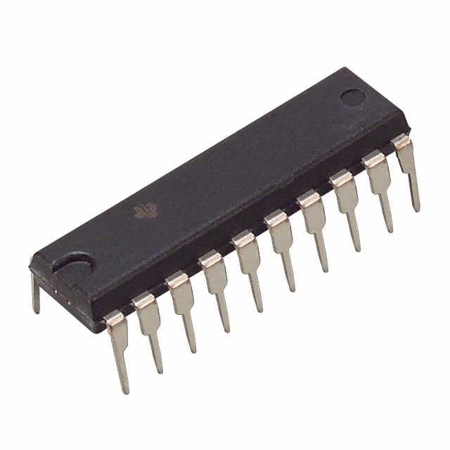
CD74HCT273EG4
Product Overview
Category
CD74HCT273EG4 belongs to the category of integrated circuits (ICs).
Use
It is commonly used in digital electronic systems for various applications such as data storage, memory units, and sequential logic circuits.
Characteristics
- CD74HCT273EG4 is a high-speed octal D-type flip-flop with reset.
- It operates at a voltage range of 2V to 6V.
- The device has a wide operating temperature range of -40°C to +85°C.
- It offers high noise immunity due to its Schmitt-trigger inputs.
- CD74HCT273EG4 provides balanced propagation delays and symmetrical output characteristics.
Package
The CD74HCT273EG4 is available in a standard 20-pin TSSOP (Thin Shrink Small Outline Package) package.
Essence
The essence of CD74HCT273EG4 lies in its ability to store and manipulate digital information in electronic systems. It serves as a fundamental building block for various digital circuits.
Packaging/Quantity
The CD74HCT273EG4 is typically packaged in reels or tubes, containing a quantity of 250 or 2000 units per package, respectively.
Specifications
- Supply Voltage Range: 2V to 6V
- Operating Temperature Range: -40°C to +85°C
- Input Voltage High: 2V (minimum), 6V (maximum)
- Input Voltage Low: 0.8V (minimum), 1.5V (maximum)
- Output Voltage High: 4.4V (minimum), VCC (maximum)
- Output Voltage Low: 0.1V (maximum), 0.1V (maximum)
- Propagation Delay Time: 15ns (typical)
Detailed Pin Configuration
The CD74HCT273EG4 has a total of 20 pins, each serving a specific function. The pin configuration is as follows:
- CLR (Clear)
- D0 (Data Input 0)
- D1 (Data Input 1)
- D2 (Data Input 2)
- D3 (Data Input 3)
- D4 (Data Input 4)
- D5 (Data Input 5)
- D6 (Data Input 6)
- D7 (Data Input 7)
- GND (Ground)
- Q7 (Output 7)
- Q6 (Output 6)
- Q5 (Output 5)
- Q4 (Output 4)
- Q3 (Output 3)
- Q2 (Output 2)
- Q1 (Output 1)
- Q0 (Output 0)
- CP (Clock Pulse)
- VCC (Supply Voltage)
Functional Features
- CD74HCT273EG4 is equipped with a synchronous clock input (CP) and an asynchronous clear input (CLR).
- It can store data on the rising edge of the clock signal.
- The device offers a reset function that allows all outputs to be cleared simultaneously.
- CD74HCT273EG4 provides eight individual flip-flops, allowing independent storage of data.
Advantages and Disadvantages
Advantages
- High-speed operation enables efficient data processing.
- Wide operating temperature range makes it suitable for various environments.
- Schmitt-trigger inputs provide high noise immunity.
- Balanced propagation delays ensure reliable performance.
Disadvantages
- Limited voltage supply range (2V to 6V).
- Requires external components for proper functioning in complex circuits.
Working Principles
CD74HCT273EG4 operates based on the principles of flip-flops and sequential logic circuits. It stores data on the rising edge of the clock signal and retains it until a new input is received or the clear input is activated.
Detailed Application Field Plans
CD74HCT273EG4 finds applications in various digital electronic systems, including but not limited to: - Microcontrollers - Data storage devices - Memory units - Counters and registers - Address decoders
Detailed and Complete Alternative Models
Some alternative models that can be considered as alternatives to CD74HCT273EG4 are: - SN74HCT273N - MC74HCT273AN - 74HCT273D
These models offer similar functionality and characteristics, providing flexibility in choosing the most suitable option for specific applications.
Word count: 529 words
Senaraikan 10 soalan dan jawapan biasa yang berkaitan dengan aplikasi CD74HCT273EG4 dalam penyelesaian teknikal
Sure! Here are 10 common questions and answers related to the application of CD74HCT273EG4 in technical solutions:
Q: What is CD74HCT273EG4? A: CD74HCT273EG4 is a high-speed octal D-type flip-flop with reset, manufactured by Texas Instruments.
Q: What is the purpose of CD74HCT273EG4? A: CD74HCT273EG4 is used as a storage element in digital circuits to store and control data.
Q: What is the maximum operating frequency of CD74HCT273EG4? A: The maximum operating frequency of CD74HCT273EG4 is typically around 80 MHz.
Q: How many flip-flops are there in CD74HCT273EG4? A: CD74HCT273EG4 consists of 8 individual D-type flip-flops.
Q: What is the voltage supply range for CD74HCT273EG4? A: CD74HCT273EG4 operates with a voltage supply range of 4.5V to 5.5V.
Q: Can CD74HCT273EG4 be used in both synchronous and asynchronous applications? A: Yes, CD74HCT273EG4 can be used in both synchronous and asynchronous applications.
Q: What is the output drive capability of CD74HCT273EG4? A: CD74HCT273EG4 has a typical output drive capability of ±4 mA.
Q: Does CD74HCT273EG4 have an active-low reset input? A: Yes, CD74HCT273EG4 has an active-low asynchronous reset input (CLR).
Q: Can CD74HCT273EG4 be cascaded to create larger storage registers? A: Yes, multiple CD74HCT273EG4 flip-flops can be cascaded together to create larger storage registers.
Q: What is the package type of CD74HCT273EG4? A: CD74HCT273EG4 is available in a 20-pin TSSOP (Thin Shrink Small Outline Package) package.
Please note that these answers are general and may vary depending on specific datasheet specifications or application requirements.


