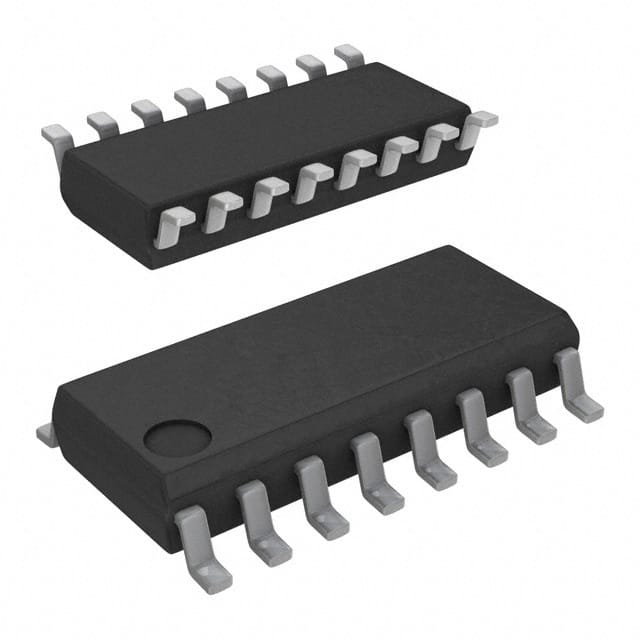
CD74HC4049MT
Product Overview
- Category: Integrated Circuit
- Use: Logic Level Shifter
- Characteristics: High-Speed CMOS, Hex Inverting Buffer/Converter
- Package: TSSOP (Thin Shrink Small Outline Package)
- Essence: The CD74HC4049MT is a high-speed CMOS logic level shifter that features six hex inverting buffer/converter gates. It is designed to convert logic levels from one voltage to another, making it suitable for interfacing between different logic families or voltage domains.
- Packaging/Quantity: The CD74HC4049MT is typically available in reels or tubes and comes in a quantity of 2500 units per reel/tube.
Specifications
- Supply Voltage Range: 2V to 6V
- Input Voltage Range: 0V to VCC
- Output Voltage Range: 0V to VCC
- Maximum Operating Frequency: 50MHz
- Propagation Delay: 10ns (typical)
- Input Capacitance: 3.5pF (typical)
- Output Current: ±25mA
Detailed Pin Configuration
The CD74HC4049MT has a total of 16 pins arranged in a TSSOP package. The pin configuration is as follows:
- Pin 1: Input A1
- Pin 2: Output Y1
- Pin 3: Input A2
- Pin 4: Output Y2
- Pin 5: Input A3
- Pin 6: Output Y3
- Pin 7: GND (Ground)
- Pin 8: Output Y4
- Pin 9: Input A4
- Pin 10: Output Y5
- Pin 11: Input A5
- Pin 12: Output Y6
- Pin 13: VCC (Supply Voltage)
- Pin 14: Input A6
- Pin 15: Output Y7
- Pin 16: NC (No Connection)
Functional Features
- High-Speed CMOS technology allows for fast switching and high-frequency operation.
- Hex inverting buffer/converter gates provide logic level shifting capabilities.
- Wide supply voltage range enables compatibility with various systems.
- Low power consumption makes it suitable for battery-powered devices.
- Schmitt-trigger inputs ensure noise immunity and signal integrity.
Advantages and Disadvantages
Advantages: - Fast propagation delay allows for quick signal processing. - Versatile logic level shifting capabilities enable interfacing between different voltage domains. - Compact TSSOP package offers space-saving benefits. - Wide supply voltage range provides flexibility in system integration.
Disadvantages: - Limited output current may restrict usage in high-current applications. - Non-inverting buffer/converter gates are not available in this specific model.
Working Principles
The CD74HC4049MT operates based on the principles of CMOS logic. It utilizes hex inverting buffer/converter gates to convert logic levels from one voltage to another. When an input signal is applied, the gate inverts the signal and outputs the inverted result. The device is powered by a supply voltage within the specified range, which ensures proper operation of the internal circuitry.
Detailed Application Field Plans
The CD74HC4049MT finds application in various fields where logic level shifting is required. Some potential application areas include:
- Microcontroller Interfacing: The CD74HC4049MT can be used to interface microcontrollers operating at different voltage levels, allowing seamless communication between them.
- Sensor Networks: In sensor networks, where different sensors may operate at different voltage levels, the CD74HC4049MT can be employed to bridge the gap and enable data exchange.
- Industrial Automation: The device can be utilized in industrial automation systems to interface between different logic families used in control circuits, ensuring compatibility and reliable operation.
Detailed and Complete Alternative Models
- CD74HC4049E: This model is similar to the CD74HC4049MT but comes in a DIP (Dual Inline Package) instead of a TSSOP package.
- CD74HCT4049M: This model is a high-speed CMOS logic level shifter with Schmitt-trigger inputs, offering enhanced noise immunity.
- SN74HC4049N: This model is another hex inverting buffer/converter gate IC that operates at a wide supply voltage range and comes in a DIP package.
(Note: The above alternative models are just a few examples and not an exhaustive list.)
Word count: 511 words
Senaraikan 10 soalan dan jawapan biasa yang berkaitan dengan aplikasi CD74HC4049MT dalam penyelesaian teknikal
Sure! Here are 10 common questions and answers related to the application of CD74HC4049MT in technical solutions:
Q: What is CD74HC4049MT? A: CD74HC4049MT is a hex inverter/buffer IC (integrated circuit) that can be used for signal amplification, level shifting, and logic inversion.
Q: What is the voltage supply range for CD74HC4049MT? A: The voltage supply range for CD74HC4049MT is typically between 2V and 6V.
Q: Can CD74HC4049MT be used for level shifting between different voltage domains? A: Yes, CD74HC4049MT can be used for level shifting between different voltage domains as long as the voltage levels are within its specified range.
Q: How many inverters are there in CD74HC4049MT? A: CD74HC4049MT contains six independent inverters.
Q: What is the maximum output current of CD74HC4049MT? A: The maximum output current of CD74HC4049MT is typically around 5mA.
Q: Can CD74HC4049MT be used for driving capacitive loads? A: Yes, CD74HC4049MT can drive small capacitive loads, but it is recommended to use an external buffer or driver for larger capacitive loads.
Q: What is the propagation delay of CD74HC4049MT? A: The propagation delay of CD74HC4049MT is typically around 15ns.
Q: Is CD74HC4049MT suitable for high-speed applications? A: CD74HC4049MT is not specifically designed for high-speed applications, but it can be used in moderate-speed digital circuits.
Q: Can CD74HC4049MT be used for analog signal processing? A: No, CD74HC4049MT is primarily designed for digital signal processing and logic functions. It is not recommended for analog signal processing.
Q: What is the package type of CD74HC4049MT? A: CD74HC4049MT is available in a surface-mount SOIC (Small Outline Integrated Circuit) package.
Please note that these answers are general and may vary depending on specific datasheet specifications and application requirements.


