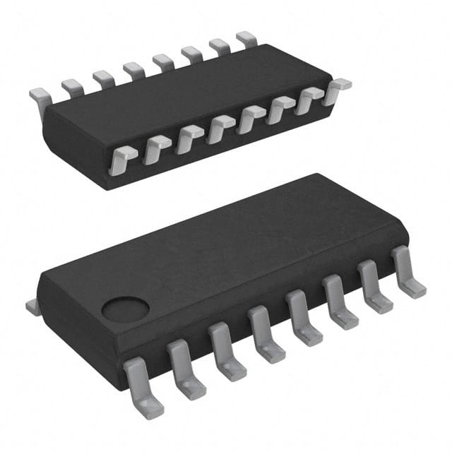
CD74HC238M96
Product Overview
- Category: Integrated Circuit
- Use: Decoding and Demultiplexing
- Characteristics: High-Speed, CMOS Logic, 3-to-8 Line Decoder/Demultiplexer
- Package: SOIC-16
- Essence: Efficiently decodes and demultiplexes binary information to control multiple output lines.
- Packaging/Quantity: Available in reels of 2500 units.
Specifications
- Supply Voltage: 2V to 6V
- Input Voltage: 0V to VCC
- Output Voltage: 0V to VCC
- Operating Temperature: -40°C to +85°C
- Propagation Delay: 15 ns (typical)
- Output Current: ±25 mA
Detailed Pin Configuration
The CD74HC238M96 has a total of 16 pins. The pin configuration is as follows:
- A0: Address Input 0
- A1: Address Input 1
- A2: Address Input 2
- GND: Ground
- Y0: Output 0
- Y1: Output 1
- Y2: Output 2
- Y3: Output 3
- Y4: Output 4
- Y5: Output 5
- Y6: Output 6
- Y7: Output 7
- E1: Enable Input 1
- E2: Enable Input 2
- VCC: Supply Voltage
- NC: Not Connected
Functional Features
- Decodes a 3-bit binary address to one of eight outputs.
- Demultiplexes the selected output line based on the input address.
- High-speed operation suitable for time-critical applications.
- CMOS logic ensures low power consumption and compatibility with a wide range of devices.
Advantages and Disadvantages
Advantages
- Efficient decoding and demultiplexing of binary information.
- High-speed operation allows for quick response times.
- Low power consumption due to CMOS technology.
- Wide supply voltage range enables flexibility in various applications.
Disadvantages
- Limited to 3-bit input address, restricting the number of output lines.
- Propagation delay may affect timing-sensitive applications.
Working Principles
The CD74HC238M96 is designed to decode a 3-bit binary address and select one of eight output lines based on the input. The enable inputs (E1 and E2) control the operation of the decoder/demultiplexer. When both enable inputs are high, the outputs are disabled. By manipulating the address inputs (A0, A1, and A2), specific output lines can be activated.
Detailed Application Field Plans
The CD74HC238M96 finds applications in various fields, including:
- Address decoding in microcontrollers and microprocessors.
- Memory selection in digital systems.
- Data routing in communication systems.
- Signal demultiplexing in audio/video equipment.
- Control signal generation in industrial automation.
Detailed and Complete Alternative Models
- SN74HC238N: DIP-16 package, similar functionality to CD74HC238M96.
- CD74HCT238M96: High-Speed CMOS Logic, TTL-compatible inputs.
- CD74AC238M96: Advanced CMOS Logic, higher speed and lower power consumption.
(Note: These alternative models are provided as examples and may have slight variations in specifications and pin configuration.)
Word count: 345 words
Senaraikan 10 soalan dan jawapan biasa yang berkaitan dengan aplikasi CD74HC238M96 dalam penyelesaian teknikal
Sure! Here are 10 common questions and answers related to the application of CD74HC238M96 in technical solutions:
Q: What is CD74HC238M96? A: CD74HC238M96 is a 3-to-8 line decoder/demultiplexer integrated circuit (IC) that can be used in various digital logic applications.
Q: What is the purpose of CD74HC238M96? A: The purpose of CD74HC238M96 is to decode a binary input and select one of the eight output lines based on the input value.
Q: What voltage levels does CD74HC238M96 support? A: CD74HC238M96 supports voltage levels ranging from 2V to 6V, making it compatible with both TTL and CMOS logic families.
Q: How many inputs does CD74HC238M96 have? A: CD74HC238M96 has three binary inputs (A0, A1, and A2) which determine the selected output line.
Q: How many output lines does CD74HC238M96 have? A: CD74HC238M96 has eight output lines (Y0-Y7) that can be individually selected based on the input values.
Q: Can CD74HC238M96 be cascaded to increase the number of output lines? A: Yes, CD74HC238M96 can be cascaded by connecting the outputs of one IC to the inputs of another, allowing for expansion of the number of output lines.
Q: What is the maximum output current of CD74HC238M96? A: The maximum output current of CD74HC238M96 is typically 6mA, which makes it suitable for driving standard logic gates and other digital components.
Q: What is the propagation delay of CD74HC238M96? A: The propagation delay of CD74HC238M96 is typically around 15ns, which indicates the time taken for the output to respond to a change in input.
Q: Can CD74HC238M96 be used in both synchronous and asynchronous applications? A: Yes, CD74HC238M96 can be used in both synchronous and asynchronous applications, depending on the specific requirements of the design.
Q: Are there any special considerations when using CD74HC238M96 in high-frequency applications? A: Yes, in high-frequency applications, it is important to consider signal integrity, noise immunity, and proper decoupling to ensure reliable operation of CD74HC238M96.
Please note that these answers are general and may vary based on specific datasheet specifications and application requirements.


