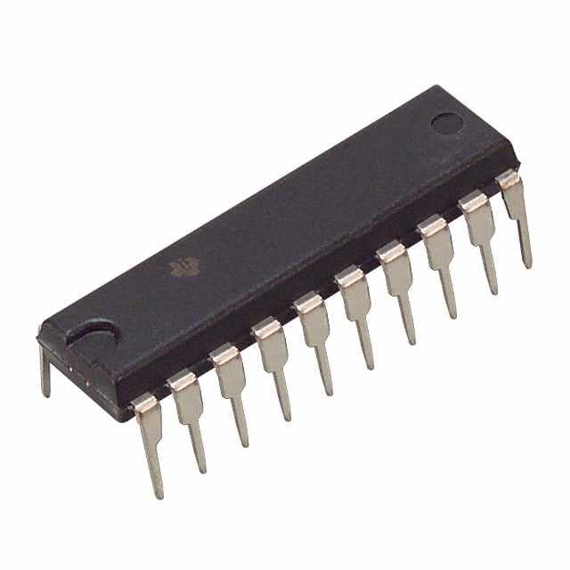
CD74AC541EG4
Product Overview
- Category: Integrated Circuit (IC)
- Use: Buffer/Line Driver
- Characteristics: High-speed, low-power, octal buffer with 3-state outputs
- Package: SOIC (Small Outline Integrated Circuit)
- Essence: Provides a high-performance buffer solution for digital systems
- Packaging/Quantity: Tape and Reel, 2500 pieces per reel
Specifications
- Supply Voltage Range: 2V to 6V
- Input Voltage Range: 0V to VCC
- Output Voltage Range: 0V to VCC
- Maximum Operating Frequency: 100MHz
- Number of Buffers: 8
- Output Drive Capability: ±24mA
- Propagation Delay Time: 5.5ns (typical)
Detailed Pin Configuration
The CD74AC541EG4 has a total of 20 pins, which are arranged as follows:
- GND (Ground)
- A1 (Input A1)
- B1 (Input B1)
- Y1 (Output Y1)
- A2 (Input A2)
- B2 (Input B2)
- Y2 (Output Y2)
- A3 (Input A3)
- B3 (Input B3)
- Y3 (Output Y3)
- A4 (Input A4)
- B4 (Input B4)
- Y4 (Output Y4)
- VCC (Positive Power Supply)
- OE (Output Enable)
- Y5 (Output Y5)
- A5 (Input A5)
- B5 (Input B5)
- Y6 (Output Y6)
- A6 (Input A6)
Functional Features
- Octal buffer with 3-state outputs
- Non-inverting buffer
- High-speed operation
- Low power consumption
- Schmitt-trigger inputs for noise immunity
- Output enable control for easy interfacing with other devices
Advantages and Disadvantages
Advantages: - High-speed operation allows for efficient data transfer - Low power consumption helps in reducing overall system energy requirements - Schmitt-trigger inputs provide noise immunity, ensuring reliable signal processing - Output enable control simplifies interfacing with other devices
Disadvantages: - Limited output drive capability may not be suitable for high-current applications - Restricted voltage range (2V to 6V) may limit compatibility with certain systems
Working Principles
The CD74AC541EG4 is an octal buffer IC that amplifies and buffers digital signals. It operates by receiving input signals on the A1-A6 pins and B1-B5 pins, which are then amplified and transmitted to the corresponding Y1-Y6 output pins. The OE pin controls the output enable function, allowing the user to enable or disable the outputs as needed.
Detailed Application Field Plans
The CD74AC541EG4 is commonly used in various digital systems where buffering and line driving capabilities are required. Some of its typical application fields include:
- Microprocessors: The IC can be used to interface microprocessors with other peripheral devices, ensuring proper signal levels and driving capability.
- Memory Systems: It can be employed in memory modules to amplify and buffer address and data signals, facilitating reliable communication between the memory and the processor.
- Communication Systems: The IC finds utility in communication systems, such as routers and switches, to enhance signal integrity and drive signals across different network interfaces.
- Industrial Automation: It can be utilized in industrial automation systems to buffer and drive control signals, ensuring accurate and timely operation of various components.
Detailed and Complete Alternative Models
Some alternative models that offer similar functionality to the CD74AC541EG4 include:
- SN74AC541: Manufactured by Texas Instruments, this octal buffer IC offers similar features and performance characteristics.
- MC74AC541: Produced by ON Semiconductor, this IC is another alternative that provides octal buffering capabilities.
- 74HC541: This IC from NXP Semiconductors is a popular alternative with comparable specifications and pin configuration.
These alternative models can be considered based on specific requirements and availability in the market.
Word count: 536 words
Senaraikan 10 soalan dan jawapan biasa yang berkaitan dengan aplikasi CD74AC541EG4 dalam penyelesaian teknikal
Sure! Here are 10 common questions and answers related to the application of CD74AC541EG4 in technical solutions:
Q: What is CD74AC541EG4? A: CD74AC541EG4 is a type of octal buffer/line driver integrated circuit (IC) that can be used for signal amplification, buffering, and level shifting.
Q: What is the voltage supply range for CD74AC541EG4? A: CD74AC541EG4 operates with a voltage supply range of 2V to 6V.
Q: How many input/output pins does CD74AC541EG4 have? A: CD74AC541EG4 has 8 input pins and 8 output pins, making it an octal device.
Q: What is the maximum output current of CD74AC541EG4? A: The maximum output current of CD74AC541EG4 is typically around 24mA.
Q: Can CD74AC541EG4 handle bidirectional data flow? A: Yes, CD74AC541EG4 supports bidirectional data flow, allowing it to be used for both input and output applications.
Q: Is CD74AC541EG4 compatible with TTL logic levels? A: Yes, CD74AC541EG4 is compatible with TTL (Transistor-Transistor Logic) logic levels, making it suitable for interfacing with TTL devices.
Q: What is the propagation delay of CD74AC541EG4? A: The propagation delay of CD74AC541EG4 is typically around 6ns.
Q: Can CD74AC541EG4 drive capacitive loads? A: Yes, CD74AC541EG4 can drive capacitive loads up to a certain limit. It is recommended to refer to the datasheet for specific details.
Q: What is the temperature range for CD74AC541EG4? A: CD74AC541EG4 can operate within a temperature range of -40°C to 85°C.
Q: Can CD74AC541EG4 be used in high-speed applications? A: Yes, CD74AC541EG4 is designed for high-speed operation and can be used in various high-frequency applications.
Please note that these answers are general and may vary depending on the specific datasheet and manufacturer's specifications.


