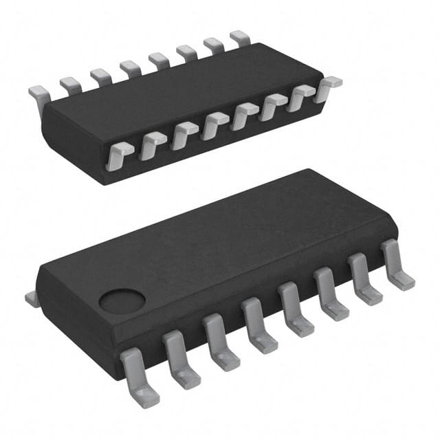
CD4050BDE4
Product Overview
Category
CD4050BDE4 belongs to the category of integrated circuits (ICs).
Use
The CD4050BDE4 is a hex non-inverting buffer and converter IC. It is commonly used for level shifting, signal buffering, and voltage conversion applications.
Characteristics
- Hex non-inverting buffer and converter
- Wide supply voltage range: 3V to 18V
- High sink/source current capability: ±6mA
- Low power consumption
- High noise immunity
- Fast switching speed
Package
CD4050BDE4 is available in a standard 16-pin SOIC (Small Outline Integrated Circuit) package.
Essence
The essence of CD4050BDE4 lies in its ability to provide non-inverting buffering and voltage conversion functions, making it an essential component in various electronic circuits.
Packaging/Quantity
CD4050BDE4 is typically packaged in reels or tubes, with quantities varying depending on the manufacturer's specifications.
Specifications
- Supply Voltage Range: 3V to 18V
- Input Voltage Range: GND to VDD
- Output Voltage Range: GND to VDD
- Maximum Input Current: ±10µA
- Maximum Quiescent Supply Current: 1µA
- Operating Temperature Range: -55°C to +125°C
Detailed Pin Configuration
The CD4050BDE4 has a total of 16 pins, numbered as follows:
- A1
- B1
- Y1
- A2
- B2
- Y2
- A3
- B3
- Y3
- A4
- B4
- Y4
- A5
- B5
- Y5
- VDD
Functional Features
- Non-inverting buffer and converter
- High input impedance
- Low output impedance
- Wide supply voltage range
- High noise immunity
- Fast switching speed
- High sink/source current capability
Advantages and Disadvantages
Advantages
- Versatile and widely used in various applications
- Wide supply voltage range allows for compatibility with different systems
- High noise immunity ensures reliable signal transmission
- Fast switching speed enables efficient data processing
Disadvantages
- Limited number of input/output channels (6 in total)
- Not suitable for high-frequency applications
Working Principles
The CD4050BDE4 operates based on the principles of non-inverting buffering and voltage conversion. It takes an input signal and provides a non-inverted output signal with increased current capability. The IC uses a combination of transistors and logic gates to achieve this functionality.
Detailed Application Field Plans
CD4050BDE4 finds applications in various fields, including but not limited to:
- Level shifting in digital circuits
- Signal buffering in communication systems
- Voltage conversion in power supply circuits
- Logic level translation in microcontroller interfacing
- Signal conditioning in sensor interfaces
Detailed and Complete Alternative Models
Some alternative models that can be considered as alternatives to CD4050BDE4 are:
- CD4049UBE
- SN74HC4050N
- MC14050BCP
- HEF4050BP
- TC4050BF
These alternatives offer similar functionality and can be used interchangeably depending on specific requirements.
In conclusion, the CD4050BDE4 is a versatile hex non-inverting buffer and converter IC widely used in various electronic applications. Its characteristics, functional features, advantages, and disadvantages make it a valuable component in signal processing and voltage conversion circuits.
Senaraikan 10 soalan dan jawapan biasa yang berkaitan dengan aplikasi CD4050BDE4 dalam penyelesaian teknikal
Sure! Here are 10 common questions and answers related to the application of CD4050BDE4 in technical solutions:
Q: What is CD4050BDE4? A: CD4050BDE4 is a hex non-inverting buffer and converter IC (integrated circuit) commonly used for level shifting, signal buffering, and voltage conversion applications.
Q: What is the operating voltage range of CD4050BDE4? A: CD4050BDE4 operates within a voltage range of 3V to 18V.
Q: Can CD4050BDE4 be used for logic level shifting? A: Yes, CD4050BDE4 can be used for logic level shifting as it provides high-to-low or low-to-high voltage translation.
Q: How many channels does CD4050BDE4 have? A: CD4050BDE4 has six channels, allowing it to handle multiple signals simultaneously.
Q: What is the maximum output current of CD4050BDE4? A: The maximum output current of CD4050BDE4 is typically around 6mA.
Q: Can CD4050BDE4 be used for interfacing between different voltage domains? A: Yes, CD4050BDE4 is commonly used for interfacing between different voltage domains, ensuring compatibility between different components.
Q: Is CD4050BDE4 suitable for bidirectional level shifting? A: No, CD4050BDE4 is unidirectional and can only perform level shifting in one direction.
Q: What is the typical propagation delay of CD4050BDE4? A: The typical propagation delay of CD4050BDE4 is around 60ns.
Q: Can CD4050BDE4 be used for voltage level conversion in I2C communication? A: Yes, CD4050BDE4 can be used to convert voltage levels between devices communicating via I2C protocol.
Q: What are some common applications of CD4050BDE4? A: CD4050BDE4 is commonly used in applications such as level shifting in mixed-voltage systems, interfacing between different logic families, signal buffering, and voltage translation in various electronic circuits.
Please note that the answers provided here are general and may vary depending on specific use cases and requirements.


