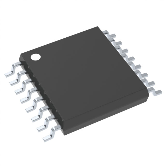
CD4009UBPW
Basic Information Overview
- Category: Integrated Circuit (IC)
- Use: Logic Inverter/Buffer
- Characteristics: Hex Inverting Buffer/Converter, High Voltage Tolerant Inputs, Wide Operating Voltage Range
- Package: TSSOP (Thin Shrink Small Outline Package)
- Essence: Hex inverting buffer/converter with high voltage tolerance and wide operating voltage range
- Packaging/Quantity: Tape and Reel, 2500 units per reel
Specifications
- Supply Voltage Range: 3V to 18V
- Input Voltage Range: 0V to VDD
- Output Voltage Range: 0V to VDD
- Maximum Input Current: ±10mA
- Maximum Output Current: ±25mA
- Propagation Delay Time: 60ns (typical)
Detailed Pin Configuration
The CD4009UBPW has a total of 16 pins. The pin configuration is as follows:
Pin 1: Input A1
Pin 2: Output Y1
Pin 3: Input A2
Pin 4: Output Y2
Pin 5: Input A3
Pin 6: Output Y3
Pin 7: GND (Ground)
Pin 8: Output Y4
Pin 9: Input A4
Pin 10: Output Y5
Pin 11: Input A5
Pin 12: Output Y6
Pin 13: VDD (Supply Voltage)
Pin 14: Input A6
Pin 15: Output Y7
Pin 16: Input A7
Functional Features
- Hex Inverting Buffer/Converter: The CD4009UBPW consists of six independent inverters that can be used for logic inversion or buffering purposes.
- High Voltage Tolerant Inputs: The inputs of the CD4009UBPW can tolerate voltages higher than the supply voltage, making it suitable for use in applications with varying input voltage levels.
- Wide Operating Voltage Range: The IC can operate within a wide range of supply voltages, from 3V to 18V.
Advantages and Disadvantages
Advantages: - Versatile hex inverting buffer/converter - High voltage tolerance - Wide operating voltage range
Disadvantages: - Relatively slow propagation delay time compared to some other ICs - Limited output current capability
Working Principles
The CD4009UBPW is based on complementary metal-oxide-semiconductor (CMOS) technology. Each inverter within the IC consists of a PMOS transistor and an NMOS transistor. When the input voltage is low, the PMOS transistor conducts and the NMOS transistor is off, resulting in a high output voltage. Conversely, when the input voltage is high, the PMOS transistor is off and the NMOS transistor conducts, leading to a low output voltage.
Detailed Application Field Plans
The CD4009UBPW can be used in various applications, including: 1. Logic level shifting: It can be used to convert logic signals between different voltage levels. 2. Signal inversion: It can invert logic signals, changing a high input to a low output and vice versa. 3. Buffering: It can be used to isolate or amplify logic signals, providing sufficient driving capability for downstream components.
Detailed and Complete Alternative Models
Some alternative models that offer similar functionality to the CD4009UBPW are: - CD4049UB: Hex Inverting Buffer/Converter with Open-Drain Outputs - CD4069UB: Hex Inverter with High-Voltage Tolerance - MC14069UB: Hex Inverter/Buffer with Schmitt Trigger Inputs
These alternative models provide similar features and can be used as substitutes depending on specific application requirements.
Word count: 345 words
Senaraikan 10 soalan dan jawapan biasa yang berkaitan dengan aplikasi CD4009UBPW dalam penyelesaian teknikal
Sure! Here are 10 common questions and answers related to the application of CD4009UBPW in technical solutions:
Q: What is CD4009UBPW? A: CD4009UBPW is a CMOS hex inverter/buffer IC (Integrated Circuit) that can be used for various digital logic applications.
Q: What is the supply voltage range for CD4009UBPW? A: The supply voltage range for CD4009UBPW is typically between 3V and 18V.
Q: Can CD4009UBPW be used as an inverter? A: Yes, CD4009UBPW can be used as an inverter as it has six independent inverters on a single chip.
Q: What is the maximum output current of CD4009UBPW? A: The maximum output current of CD4009UBPW is typically around 6mA.
Q: Can CD4009UBPW be used for level shifting applications? A: Yes, CD4009UBPW can be used for level shifting applications as it supports a wide supply voltage range.
Q: Is CD4009UBPW suitable for high-speed applications? A: No, CD4009UBPW is not specifically designed for high-speed applications. It is more commonly used in low to moderate speed digital circuits.
Q: Can CD4009UBPW be used in battery-powered devices? A: Yes, CD4009UBPW can be used in battery-powered devices as it operates within a wide supply voltage range, including lower voltages.
Q: Does CD4009UBPW have built-in protection features? A: No, CD4009UBPW does not have built-in protection features. External protection circuitry may be required for certain applications.
Q: Can CD4009UBPW be used in both digital and analog circuits? A: CD4009UBPW is primarily designed for digital logic applications. It may not be suitable for precision analog circuits due to its inherent characteristics.
Q: Are there any specific precautions to consider when using CD4009UBPW? A: Yes, some precautions include avoiding static discharge, ensuring proper power supply decoupling, and following the recommended operating conditions mentioned in the datasheet.
Please note that these answers are general and may vary depending on the specific application and requirements. Always refer to the datasheet and consult with an expert for accurate information.


