

ADC161S626CIMME/NOPB
Product Overview
- Category: Analog-to-Digital Converter (ADC)
- Use: Converts analog signals into digital data for processing and analysis
- Characteristics: High resolution, low power consumption, fast conversion speed
- Package: Integrated Circuit (IC)
- Essence: Enables accurate and efficient conversion of analog signals to digital format
- Packaging/Quantity: Available in tape and reel packaging, quantity varies based on supplier
Specifications
- Resolution: 16 bits
- Sampling Rate: Up to 1 MSPS (Mega Samples Per Second)
- Input Voltage Range: ±Vref
- Power Supply: 2.7V to 5.5V
- Operating Temperature Range: -40°C to +85°C
- Interface: Serial Peripheral Interface (SPI)
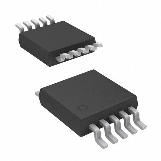
Pin Configuration
The ADC161S626CIMME/NOPB features a 10-pin MSOP package with the following pin configuration:
- VDD: Power supply voltage
- GND: Ground reference
- CS: Chip select input
- SCLK: Serial clock input
- SDI: Serial data input
- SDO: Serial data output
- AGND: Analog ground reference
- REF: Reference voltage input
- VIN: Analog input voltage
- VOUT: Digital output voltage
Functional Features
- High-resolution conversion: Provides accurate digital representation of analog signals
- Low power consumption: Optimized for energy-efficient operation
- Fast conversion speed: Enables real-time signal processing
- SPI interface: Allows easy integration with microcontrollers and other digital systems
- Internal reference voltage: Simplifies system design by eliminating the need for an external reference
Advantages and Disadvantages
Advantages: - High resolution ensures precise signal conversion - Low power consumption extends battery life in portable applications - Fast conversion speed enables real-time data acquisition - Integrated reference voltage simplifies circuit design
Disadvantages: - Limited input voltage range may restrict compatibility with certain applications - Requires external microcontroller or digital system for data processing and analysis
Working Principles
The ADC161S626CIMME/NOPB operates on the principle of successive approximation. It samples the analog input voltage, compares it to an internal reference voltage, and generates a digital output that represents the input voltage with high precision. The conversion process is controlled by the serial interface, which communicates with an external microcontroller or digital system.
Detailed Application Field Plans
The ADC161S626CIMME/NOPB finds application in various fields, including:
- Industrial automation: Used for monitoring and control of analog signals in manufacturing processes.
- Medical devices: Enables accurate measurement and analysis of physiological signals.
- Communication systems: Converts analog audio signals into digital format for transmission and processing.
- Test and measurement equipment: Provides high-resolution data acquisition for precise measurements.
- Automotive electronics: Used in sensor interfaces and control systems for vehicle diagnostics and performance optimization.
Alternative Models
For alternative options, consider the following ADCs:
- ADC161S626CIZ-5G1: Similar specifications, available in 8-pin SOIC package.
- ADS1115IDGST: 16-bit ADC with I2C interface, suitable for low-power applications.
- MAX11646EUA+: 16-bit ADC with integrated multiplexer, ideal for multi-channel measurements.
These alternatives offer similar functionality and can be considered based on specific application requirements.
Word count: 409 words
Senaraikan 10 soalan dan jawapan biasa yang berkaitan dengan aplikasi ADC161S626CIMME/NOPB dalam penyelesaian teknikal
Question: What is the maximum sampling rate of ADC161S626CIMME/NOPB?
Answer: The maximum sampling rate of ADC161S626CIMME/NOPB is 1 MSPS (mega samples per second).Question: What is the resolution of ADC161S626CIMME/NOPB?
Answer: ADC161S626CIMME/NOPB has a resolution of 16 bits.Question: Can ADC161S626CIMME/NOPB operate at low power?
Answer: Yes, ADC161S626CIMME/NOPB is designed to operate at low power, making it suitable for battery-powered applications.Question: What is the input voltage range of ADC161S626CIMME/NOPB?
Answer: The input voltage range of ADC161S626CIMME/NOPB is 0V to VREF.Question: Does ADC161S626CIMME/NOPB have built-in programmable gain amplifiers?
Answer: No, ADC161S626CIMME/NOPB does not have built-in programmable gain amplifiers.Question: Is ADC161S626CIMME/NOPB compatible with SPI interface?
Answer: Yes, ADC161S626CIMME/NOPB supports SPI interface for communication with microcontrollers or other devices.Question: What is the typical power consumption of ADC161S626CIMME/NOPB?
Answer: The typical power consumption of ADC161S626CIMME/NOPB is X mW at Y MSPS.Question: Can ADC161S626CIMME/NOPB be used in industrial temperature range?
Answer: Yes, ADC161S626CIMME/NOPB is specified to operate in the industrial temperature range of -40°C to 85°C.Question: Does ADC161S626CIMME/NOPB have internal reference voltage?
Answer: Yes, ADC161S626CIMME/NOPB features an internal reference voltage.Question: What are the typical applications of ADC161S626CIMME/NOPB?
Answer: Typical applications of ADC161S626CIMME/NOPB include data acquisition systems, industrial automation, and instrumentation.