

Lihat spesifikasi untuk butiran produk.
ADC141S625CIMMX
Product Overview
- Category: Analog-to-Digital Converter (ADC)
- Use: Converts analog signals into digital data for processing and analysis
- Characteristics: High-resolution, low-power consumption, fast conversion speed
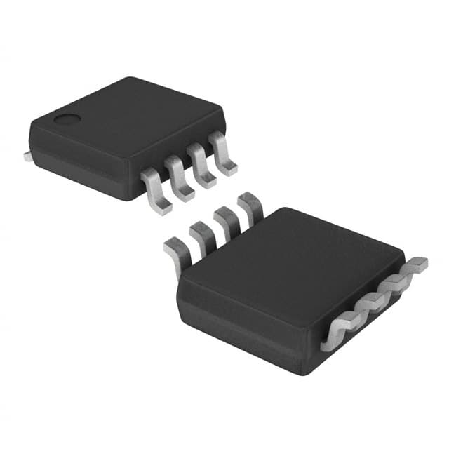
- Package: Small outline integrated circuit (SOIC)
- Essence: Provides accurate and reliable conversion of analog signals to digital format
- Packaging/Quantity: Available in reels of 2500 units
Specifications
- Resolution: 14 bits
- Sampling Rate: 625 kilosamples per second (ksps)
- Input Voltage Range: 0 to Vref
- Power Supply: 2.7V to 5.5V
- Operating Temperature Range: -40°C to +85°C
- Interface: Serial Peripheral Interface (SPI)
Pin Configuration
The ADC141S625CIMMX has a total of 16 pins arranged as follows:
- VDD: Power supply voltage
- VREF: Reference voltage input
- AGND: Analog ground
- VIN: Analog input voltage
- SCLK: Serial clock input
- DIN: Serial data input
- DOUT: Serial data output
- CS: Chip select input
- DGND: Digital ground
- SDI: Serial data interface
- SDO: Serial data output
- SCK: Serial clock
- CSB: Chip select
- SHDN: Shutdown control input
- REFSEL: Reference voltage selection
- VDD: Power supply voltage
Functional Features
- High-resolution conversion with 14-bit accuracy
- Fast sampling rate of 625 ksps allows real-time data acquisition
- Low power consumption extends battery life in portable applications
- Wide input voltage range accommodates various signal levels
- Serial Peripheral Interface (SPI) enables easy integration with microcontrollers
Advantages and Disadvantages
Advantages
- High-resolution conversion ensures accurate representation of analog signals
- Fast sampling rate allows for real-time data processing
- Low power consumption makes it suitable for battery-powered devices
- Small package size saves board space in compact designs
- Wide input voltage range provides flexibility in signal acquisition
Disadvantages
- Limited to 14-bit resolution, may not be suitable for applications requiring higher precision
- Requires an external reference voltage source for accurate conversions
- SPI interface may require additional pins and circuitry in complex systems
Working Principles
The ADC141S625CIMMX operates on the principle of successive approximation. It samples the analog input voltage and compares it to a reference voltage. The converter then generates a digital output code that represents the input voltage with high accuracy.
The device utilizes an internal clock to control the sampling and conversion process. The serial interface allows communication with a microcontroller or other digital devices for data transfer.
Detailed Application Field Plans
The ADC141S625CIMMX is commonly used in various applications, including:
- Industrial automation: Monitoring and control systems
- Medical equipment: Patient monitoring devices, diagnostic instruments
- Communications: Data acquisition and signal processing
- Automotive: Engine control units, sensor interfaces
- Consumer electronics: Audio processing, instrumentation
Detailed and Complete Alternative Models
- ADC121S021CIMM: 12-bit resolution, 21 ksps sampling rate, SOIC package
- ADC161S626CIMM: 16-bit resolution, 626 ksps sampling rate, SOIC package
- ADC081S101CIMM: 8-bit resolution, 101 ksps sampling rate, SOIC package
- ADC241S051CIMM: 24-bit resolution, 51 ksps sampling rate, SOIC package
These alternative models offer different resolutions and sampling rates to suit specific application requirements.
In conclusion, the ADC141S625CIMMX is a high-resolution analog-to-digital converter with fast conversion speed and low power consumption. Its small package size and wide input voltage range make it suitable for various applications in industrial automation, medical equipment, communications, automotive, and consumer electronics. Alternative models with different specifications are available to meet specific needs.
Senaraikan 10 soalan dan jawapan biasa yang berkaitan dengan aplikasi ADC141S625CIMMX dalam penyelesaian teknikal
Sure! Here are 10 common questions and answers related to the application of ADC141S625CIMMX in technical solutions:
Q: What is ADC141S625CIMMX? A: ADC141S625CIMMX is a specific model of Analog-to-Digital Converter (ADC) manufactured by Texas Instruments.
Q: What is the resolution of ADC141S625CIMMX? A: The ADC141S625CIMMX has a resolution of 14 bits, meaning it can convert an analog input signal into a digital value with 14 bits of precision.
Q: What is the sampling rate of ADC141S625CIMMX? A: The ADC141S625CIMMX has a maximum sampling rate of 625 kilosamples per second (ksps).
Q: What is the supply voltage range for ADC141S625CIMMX? A: The ADC141S625CIMMX operates with a supply voltage range of 2.7V to 5.25V.
Q: What is the input voltage range of ADC141S625CIMMX? A: The ADC141S625CIMMX has a differential input voltage range of -0.3V to VREF + 0.3V.
Q: Does ADC141S625CIMMX support multiple input channels? A: Yes, ADC141S625CIMMX has a total of 4 input channels, allowing you to sample multiple analog signals simultaneously.
Q: What is the interface used to communicate with ADC141S625CIMMX? A: ADC141S625CIMMX uses a Serial Peripheral Interface (SPI) for communication with microcontrollers or other devices.
Q: Can ADC141S625CIMMX operate in a low-power mode? A: Yes, ADC141S625CIMMX has a power-down mode that reduces its power consumption when not actively converting analog signals.
Q: What is the typical conversion time of ADC141S625CIMMX? A: The typical conversion time for ADC141S625CIMMX is 1.6 microseconds (µs).
Q: Are there any evaluation boards or development kits available for ADC141S625CIMMX? A: Yes, Texas Instruments provides evaluation boards and development kits specifically designed for ADC141S625CIMMX to aid in its integration into technical solutions.
Please note that these answers are general and may vary depending on the specific application and implementation of ADC141S625CIMMX.