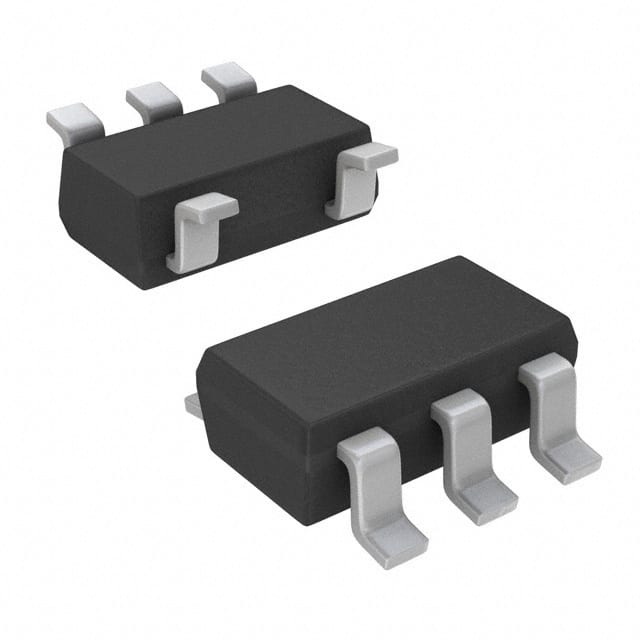
Encyclopedia Entry: 74AHCT1G125DCKRG4
Product Overview
Category
The 74AHCT1G125DCKRG4 belongs to the category of integrated circuits (ICs).
Use
This IC is commonly used for signal buffering and level shifting applications.
Characteristics
- High-speed operation
- Low power consumption
- Wide operating voltage range
- Schmitt-trigger input
- Output drive capability: ±8 mA at VCC = 5V
Package
The 74AHCT1G125DCKRG4 is available in a small SOT-353 package.
Essence
This IC serves as a single bus buffer gate with an output enable control. It provides a high-speed interface between different logic levels.
Packaging/Quantity
The 74AHCT1G125DCKRG4 is typically packaged in reels, containing a quantity of 3000 units per reel.
Specifications
- Supply Voltage Range: 4.5V to 5.5V
- Input Voltage Range: 0V to VCC
- Output Voltage Range: 0V to VCC
- Operating Temperature Range: -40°C to +85°C
- Propagation Delay Time: 6 ns (max) at VCC = 5V, TA = 25°C
Detailed Pin Configuration
The 74AHCT1G125DCKRG4 has the following pin configuration:
____
OE   |    |
A    |    |
Y    |    |
GND  |    |
VCC  |____|
- OE: Output Enable
- A: Input
- Y: Output
- GND: Ground
- VCC: Power Supply
Functional Features
- Single gate buffer with output enable control
- Provides level shifting between different logic levels
- Schmitt-trigger input for improved noise immunity
- High-speed operation allows for efficient signal buffering
Advantages and Disadvantages
Advantages
- High-speed operation enables quick signal processing
- Low power consumption for energy-efficient applications
- Wide operating voltage range allows compatibility with various systems
- Schmitt-trigger input enhances noise immunity
Disadvantages
- Limited output drive capability (±8 mA at VCC = 5V)
- Single gate functionality may not be suitable for complex applications requiring multiple gates
Working Principles
The 74AHCT1G125DCKRG4 operates as a buffer gate, amplifying and shifting the logic levels of input signals. The output enable control (OE) allows the user to enable or disable the output, providing flexibility in signal routing.
Detailed Application Field Plans
The 74AHCT1G125DCKRG4 finds application in various fields, including:
- Communication Systems: Signal buffering and level shifting in data transmission circuits.
- Industrial Automation: Interface between different logic levels in control systems.
- Consumer Electronics: Level translation in audio/video devices and portable gadgets.
- Automotive Electronics: Signal conditioning in automotive control modules.
- IoT Devices: Logic level conversion in sensor interfaces and communication modules.
Detailed and Complete Alternative Models
- SN74LVC1G125DBVR: Single bus buffer gate with output enable control from Texas Instruments.
- MC74VHC1GT125DF1G: Single gate buffer with 3-state output from ON Semiconductor.
- CD74HCT125M96: Quad bus buffer gates with 3-state outputs from Texas Instruments.
These alternative models offer similar functionality and can be considered as substitutes for the 74AHCT1G125DCKRG4.
Word count: 514 words
Senaraikan 10 soalan dan jawapan biasa yang berkaitan dengan aplikasi 74AHCT1G125DCKRG4 dalam penyelesaian teknikal
Sure! Here are 10 common questions and answers related to the application of 74AHCT1G125DCKRG4 in technical solutions:
1. What is the 74AHCT1G125DCKRG4? - The 74AHCT1G125DCKRG4 is a single bus buffer gate with 3-state output, designed for use in various digital logic applications.
2. What is the voltage range supported by 74AHCT1G125DCKRG4? - The 74AHCT1G125DCKRG4 supports a voltage range of 4.5V to 5.5V.
3. What is the maximum output current of 74AHCT1G125DCKRG4? - The maximum output current of 74AHCT1G125DCKRG4 is typically 8mA.
4. Can 74AHCT1G125DCKRG4 be used as a level shifter? - Yes, 74AHCT1G125DCKRG4 can be used as a level shifter to convert signals between different voltage levels.
5. What is the propagation delay of 74AHCT1G125DCKRG4? - The propagation delay of 74AHCT1G125DCKRG4 is typically around 6 ns.
6. Is 74AHCT1G125DCKRG4 compatible with other logic families? - Yes, 74AHCT1G125DCKRG4 is compatible with a wide range of logic families, including TTL, CMOS, and LVTTL.
7. Can 74AHCT1G125DCKRG4 be used in high-speed applications? - Yes, 74AHCT1G125DCKRG4 can be used in high-speed applications due to its fast switching speed and low propagation delay.
8. What is the power supply voltage required for 74AHCT1G125DCKRG4? - The power supply voltage required for 74AHCT1G125DCKRG4 is typically 5V.
9. Can 74AHCT1G125DCKRG4 be used in automotive applications? - Yes, 74AHCT1G125DCKRG4 is suitable for automotive applications as it meets the necessary standards and specifications.
10. Are there any recommended operating conditions for 74AHCT1G125DCKRG4? - Yes, some recommended operating conditions for 74AHCT1G125DCKRG4 include a temperature range of -40°C to +85°C and a maximum input rise and fall time of 1000 ns.
Please note that these answers are general and may vary depending on the specific datasheet and manufacturer's recommendations for the 74AHCT1G125DCKRG4.


