

74LX1G126STR
Basic Information Overview
- Category: Integrated Circuit (IC)
- Use: Logic Gate Buffer/Driver
- Characteristics: Single gate, non-inverting, tri-state output
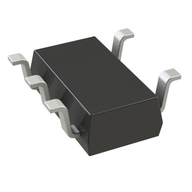
- Package: SOT-23-5
- Essence: Buffering and driving signals in digital circuits
- Packaging/Quantity: Tape and reel, 3000 units per reel
Specifications
- Supply Voltage Range: 1.65V to 5.5V
- Input Voltage Range: 0V to Vcc
- Output Voltage Range: 0V to Vcc
- Maximum Operating Frequency: 125 MHz
- Propagation Delay: 4.8 ns (typical)
- Output Drive Capability: ±24 mA
Detailed Pin Configuration
The 74LX1G126STR IC has a total of 5 pins arranged as follows: 1. Pin 1: Input (A) 2. Pin 2: Enable (E) 3. Pin 3: Ground (GND) 4. Pin 4: Output (Y) 5. Pin 5: Power Supply (Vcc)
Functional Features
- Non-inverting buffer with tri-state output
- High-speed operation suitable for various digital applications
- Wide supply voltage range allows compatibility with different systems
- Low power consumption
- ESD protection on all inputs and outputs
Advantages and Disadvantages
Advantages: - Small package size enables space-efficient designs - Tri-state output allows multiple devices to share a common bus - Wide supply voltage range enhances versatility - ESD protection ensures robustness against electrostatic discharges
Disadvantages: - Limited output drive capability may not be suitable for high-current applications - Propagation delay may affect timing-sensitive circuits
Working Principles
The 74LX1G126STR is a logic gate buffer/driver that amplifies and shapes digital signals. It operates by receiving an input signal (A) and, based on the enable signal (E), either passes the amplified signal to the output pin (Y) or enters a high-impedance state where the output is effectively disconnected from the circuit. This tri-state feature allows multiple devices to share a common bus without interfering with each other.
Detailed Application Field Plans
The 74LX1G126STR IC finds applications in various digital systems, including but not limited to: - Microcontrollers and microprocessors - Communication systems - Data storage devices - Industrial automation - Consumer electronics
Detailed and Complete Alternative Models
Some alternative models that can be considered as alternatives to the 74LX1G126STR are: - SN74LVC1G126DBVR - MC74VHC1G126DF1G - TC7SZ126AFK(TE85L,F)
These alternatives offer similar functionality and characteristics, providing options for different design requirements.
Word count: 305 words
Senaraikan 10 soalan dan jawapan biasa yang berkaitan dengan aplikasi 74LX1G126STR dalam penyelesaian teknikal
Sure! Here are 10 common questions and answers related to the application of 74LX1G126STR in technical solutions:
Q1: What is the 74LX1G126STR? A1: The 74LX1G126STR is a single bus buffer gate with three-state output, commonly used in digital logic circuits.
Q2: What is the purpose of the 74LX1G126STR? A2: The purpose of this IC is to provide buffering and signal level translation between different parts of a digital circuit.
Q3: What voltage levels does the 74LX1G126STR support? A3: The 74LX1G126STR supports voltage levels from 1.65V to 5.5V, making it compatible with a wide range of digital systems.
Q4: How many inputs and outputs does the 74LX1G126STR have? A4: The 74LX1G126STR has one input and one output, along with an enable pin for three-state control.
Q5: Can the 74LX1G126STR be used as a level shifter? A5: Yes, the 74LX1G126STR can be used as a level shifter to convert signals between different voltage domains.
Q6: What is the maximum data rate supported by the 74LX1G126STR? A6: The 74LX1G126STR can support data rates up to 400 Mbps, making it suitable for high-speed digital applications.
Q7: Can the 74LX1G126STR drive capacitive loads? A7: Yes, the 74LX1G126STR can drive small capacitive loads typically found in digital circuits without requiring additional components.
Q8: Is the 74LX1G126STR compatible with other logic families? A8: Yes, the 74LX1G126STR is compatible with a wide range of logic families, including TTL, CMOS, and LVCMOS.
Q9: Can the 74LX1G126STR be used in bidirectional applications? A9: No, the 74LX1G126STR is a unidirectional buffer and cannot be used for bidirectional data transmission.
Q10: What is the package type of the 74LX1G126STR? A10: The 74LX1G126STR is available in a small SOT-23 package, which is commonly used for surface mount applications.
Please note that these answers are general and may vary depending on the specific application and requirements.