

74LX1G03STR
Basic Information Overview
- Category: Integrated Circuit (IC)
- Use: Logic Gate
- Characteristics: Single 2-Input NAND Gate
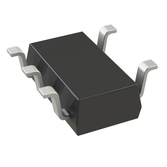
- Package: SOT-23-5
- Essence: Small-sized logic gate IC
- Packaging/Quantity: Tape and Reel, 3000 pieces per reel
Specifications
- Supply Voltage Range: 1.65V to 5.5V
- Input Voltage Range: -0.5V to VCC + 0.5V
- Output Voltage Range: -0.5V to VCC + 0.5V
- Operating Temperature Range: -40°C to +85°C
- Propagation Delay Time: 3.5ns (typical) at VCC = 3.3V, TA = 25°C
Detailed Pin Configuration
The 74LX1G03STR has a total of 5 pins: 1. Pin 1: Input A 2. Pin 2: Input B 3. Pin 3: Ground (GND) 4. Pin 4: Output Y 5. Pin 5: Power Supply (VCC)
Functional Features
- Performs logical NAND operation on two input signals (A and B)
- Provides a single output signal (Y) based on the logical operation result
- Supports wide supply voltage range for versatile applications
- Low power consumption and high-speed operation
- Compact SOT-23-5 package allows for space-efficient designs
Advantages and Disadvantages
Advantages: - Small form factor enables integration in compact electronic devices - Wide supply voltage range enhances compatibility with various systems - Low power consumption contributes to energy efficiency - High-speed operation facilitates quick signal processing
Disadvantages: - Limited number of inputs (only two) - Output current limitations may restrict use in certain applications - Sensitivity to electrostatic discharge (ESD) requires proper handling precautions
Working Principles
The 74LX1G03STR is a NAND gate, which means it performs the logical NAND operation on its two input signals. The output signal is determined by the following truth table:
| A | B | Y | |---|---|---| | 0 | 0 | 1 | | 0 | 1 | 1 | | 1 | 0 | 1 | | 1 | 1 | 0 |
The IC utilizes transistors and other electronic components to implement the logical operation, providing a reliable and efficient solution for digital circuit design.
Detailed Application Field Plans
The 74LX1G03STR can be used in various applications, including but not limited to: - Digital logic circuits - Microcontrollers and microprocessors - Communication systems - Consumer electronics - Industrial automation - Automotive electronics
Detailed and Complete Alternative Models
Some alternative models that offer similar functionality to the 74LX1G03STR include: - 74HC03: High-speed CMOS Logic Quad 2-Input NAND Gate - SN74LS00: Quadruple 2-Input Positive-NAND Gates - CD4011B: CMOS Quad 2-Input NAND Gate
These alternatives provide options with different specifications, package types, and performance characteristics, allowing designers to choose the most suitable option for their specific requirements.
Word count: 386 words
Senaraikan 10 soalan dan jawapan biasa yang berkaitan dengan aplikasi 74LX1G03STR dalam penyelesaian teknikal
Sure! Here are 10 common questions and answers related to the application of 74LX1G03STR in technical solutions:
Q1: What is the 74LX1G03STR? A1: The 74LX1G03STR is a single 2-input NAND gate IC (integrated circuit) that can be used in various electronic applications.
Q2: What is the voltage supply range for the 74LX1G03STR? A2: The voltage supply range for the 74LX1G03STR is typically between 1.65V and 5.5V.
Q3: What is the maximum output current of the 74LX1G03STR? A3: The maximum output current of the 74LX1G03STR is around 32mA.
Q4: Can the 74LX1G03STR be used as a buffer? A4: Yes, the 74LX1G03STR can be used as a buffer by connecting one input to ground and using the other input as the signal input.
Q5: What is the propagation delay of the 74LX1G03STR? A5: The propagation delay of the 74LX1G03STR is typically around 4.5ns.
Q6: Can the 74LX1G03STR be used in high-speed applications? A6: Yes, the 74LX1G03STR is designed for high-speed operation and can be used in applications that require fast switching times.
Q7: Is the 74LX1G03STR compatible with TTL logic levels? A7: Yes, the 74LX1G03STR is compatible with both TTL and CMOS logic levels.
Q8: Can the 74LX1G03STR be used in battery-powered applications? A8: Yes, the 74LX1G03STR has a low power consumption and can be used in battery-powered applications.
Q9: What is the package type of the 74LX1G03STR? A9: The 74LX1G03STR is available in a small SOT-23 package.
Q10: Can multiple 74LX1G03STR ICs be cascaded together? A10: Yes, multiple 74LX1G03STR ICs can be cascaded together to create more complex logic functions.