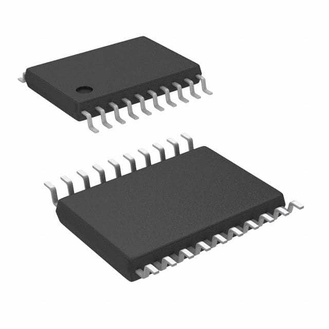
Encyclopedia Entry: 74LVX541TTR
Product Overview
Category
The 74LVX541TTR belongs to the category of integrated circuits (ICs) and specifically falls under the family of logic gates.
Use
This IC is commonly used for signal amplification, level shifting, and buffering in digital electronic circuits.
Characteristics
- Voltage Level: The 74LVX541TTR operates at a voltage level of 3.3V.
- High-Speed Operation: It offers high-speed performance, making it suitable for applications requiring quick signal processing.
- Low Power Consumption: This IC consumes low power, making it energy-efficient.
- Wide Temperature Range: It can operate within a wide temperature range, typically from -40°C to 85°C.
- RoHS Compliance: The 74LVX541TTR is compliant with the Restriction of Hazardous Substances (RoHS) directive.
Package
The 74LVX541TTR is available in a TSSOP (Thin Shrink Small Outline Package) package. This package type ensures compactness and ease of integration into circuit boards.
Essence
The essence of the 74LVX541TTR lies in its ability to provide reliable signal amplification and level shifting, enabling seamless communication between different components of a digital circuit.
Packaging/Quantity
The 74LVX541TTR is typically packaged in reels or tubes, containing a quantity of 250 or 300 units per package.
Specifications
- Logic Family: LVX
- Number of Channels: 8
- Input Voltage Range: 0V to 5.5V
- Output Voltage Range: 0V to 5.5V
- Maximum Operating Frequency: 100MHz
- Propagation Delay Time: 4.2ns (typical)
- Input Capacitance: 3.5pF (typical)
- Output Current: ±24mA
Detailed Pin Configuration
The 74LVX541TTR has a total of 20 pins, which are assigned specific functions as follows:
- GND: Ground
- A1: Input A1
- B1: Input B1
- Y1: Output Y1
- A2: Input A2
- B2: Input B2
- Y2: Output Y2
- A3: Input A3
- B3: Input B3
- Y3: Output Y3
- A4: Input A4
- B4: Input B4
- Y4: Output Y4
- VCC: Power Supply Voltage
- OE: Output Enable
- GND: Ground
- Y5: Output Y5
- B5: Input B5
- A5: Input A5
- Y6: Output Y6
Functional Features
- Signal Amplification: The 74LVX541TTR amplifies weak input signals to ensure reliable transmission.
- Level Shifting: It converts signals from one voltage level to another, facilitating compatibility between different components.
- Buffering: This IC acts as a buffer, isolating the input and output circuits to prevent interference.
Advantages and Disadvantages
Advantages
- High-speed operation allows for quick signal processing.
- Low power consumption makes it energy-efficient.
- Wide temperature range enables operation in various environments.
- RoHS compliance ensures environmental friendliness.
Disadvantages
- Limited voltage range (0V to 5.5V) may not be suitable for certain applications requiring higher voltages.
- Propagation delay time may affect real-time applications with strict timing requirements.
Working Principles
The 74LVX541TTR operates based on the principles of digital logic gates. It utilizes transistors and other electronic components to amplify, shift, and buffer signals according to the input and control signals received.
Detailed Application Field Plans
The 74LVX541TTR finds applications in various fields, including: 1. Microcontroller-based systems 2. Communication devices 3. Industrial automation 4. Automotive electronics 5. Consumer electronics
Detailed and Complete Alternative Models
Some alternative models that can be considered as alternatives to the 74LVX541TTR include: - SN74LVX541 - MC74LVX541 - CD74LVX541 - HCT541
These models offer similar functionality and can be used interchangeably depending on specific requirements.
Word count: 550 words
Senaraikan 10 soalan dan jawapan biasa yang berkaitan dengan aplikasi 74LVX541TTR dalam penyelesaian teknikal
Sure! Here are 10 common questions and answers related to the application of 74LVX541TTR in technical solutions:
Q: What is the 74LVX541TTR? A: The 74LVX541TTR is a type of octal buffer/line driver IC (integrated circuit) that can be used for signal amplification and buffering in digital circuits.
Q: What is the voltage supply range for the 74LVX541TTR? A: The 74LVX541TTR operates with a voltage supply range of 2.7V to 3.6V.
Q: How many channels does the 74LVX541TTR have? A: The 74LVX541TTR has 8 channels, making it suitable for applications requiring multiple signal lines.
Q: Can the 74LVX541TTR handle bidirectional signals? A: No, the 74LVX541TTR is a unidirectional buffer, meaning it can only amplify signals in one direction.
Q: What is the maximum output current of the 74LVX541TTR? A: The 74LVX541TTR can provide a maximum output current of 24mA per channel.
Q: Is the 74LVX541TTR compatible with TTL (Transistor-Transistor Logic) inputs? A: Yes, the 74LVX541TTR is designed to be compatible with both TTL and CMOS (Complementary Metal-Oxide-Semiconductor) inputs.
Q: Can the 74LVX541TTR tolerate overvoltage on its inputs? A: Yes, the 74LVX541TTR has input protection that allows it to tolerate voltages up to 5.5V.
Q: What is the typical propagation delay of the 74LVX541TTR? A: The typical propagation delay of the 74LVX541TTR is around 6 nanoseconds.
Q: Can the 74LVX541TTR be used in high-speed applications? A: Yes, the 74LVX541TTR is designed for high-speed operation and can be used in applications with fast switching requirements.
Q: Are there any special considerations when using the 74LVX541TTR in a PCB layout? A: It is recommended to follow proper PCB layout guidelines, such as minimizing trace lengths and providing adequate decoupling capacitors, to ensure optimal performance of the 74LVX541TTR in a circuit.
Please note that these answers are general and may vary depending on specific application requirements and datasheet specifications.


