

NLX2G14CMX1TCG
Product Overview
Category: Integrated Circuit (IC)
Use: Logic Gate
Characteristics: - Low-power Schmitt-trigger inverter - Wide supply voltage range: 1.65V to 5.5V - High noise immunity - Fast propagation delay: 4.3ns (typical) - Low power consumption: 0.9µA (typical) - Small package size: SOT-23-5
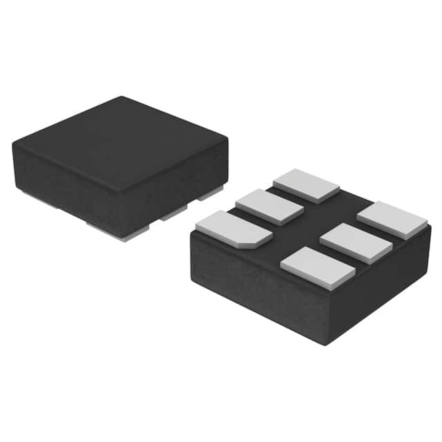
Package: SOT-23-5
Essence: The NLX2G14CMX1TCG is a low-power Schmitt-trigger inverter IC used for logic gate applications.
Packaging/Quantity: The NLX2G14CMX1TCG is available in a reel packaging with 3000 units per reel.
Specifications
- Supply Voltage Range: 1.65V to 5.5V
- Input Voltage Range: 0V to VCC
- Output Voltage Range: 0V to VCC
- Operating Temperature Range: -40°C to +85°C
- Propagation Delay: 4.3ns (typical)
- Input Capacitance: 2pF (typical)
- Power Consumption: 0.9µA (typical)
Detailed Pin Configuration
The NLX2G14CMX1TCG has the following pin configuration:
____
   A --|    |-- VCC
   B --|    |-- Y
 GND --|____|-- NC
Functional Features
- Schmitt-trigger input allows for hysteresis and improved noise immunity.
- Wide supply voltage range enables compatibility with various systems.
- Low power consumption makes it suitable for battery-powered devices.
- Fast propagation delay ensures quick response in logic circuits.
- Small package size allows for space-efficient designs.
Advantages
- High noise immunity ensures reliable operation in noisy environments.
- Wide supply voltage range provides flexibility in system integration.
- Low power consumption extends battery life in portable devices.
- Fast propagation delay enables high-speed data processing.
- Small package size saves board space in compact designs.
Disadvantages
- Limited number of inputs and outputs restricts complex circuit designs.
- Lack of built-in protection features may require additional external components.
- Sensitivity to electrostatic discharge (ESD) requires proper handling during assembly.
Working Principles
The NLX2G14CMX1TCG is based on CMOS technology, utilizing a Schmitt-trigger input. When the input voltage crosses a certain threshold level, the output switches states, providing a digital signal that corresponds to the input logic level. The Schmitt-trigger input adds hysteresis, ensuring a clean and stable output even in the presence of noise or signal fluctuations.
Detailed Application Field Plans
The NLX2G14CMX1TCG is commonly used in various applications, including:
- Digital signal processing
- Data communication systems
- Industrial automation
- Consumer electronics
- Automotive electronics
Detailed and Complete Alternative Models
Some alternative models to the NLX2G14CMX1TCG include:
- SN74LVC1G14DBVR - Single Schmitt-trigger inverter IC
- MC74VHC1GT14DF1G - Single Schmitt-trigger inverter IC
- 74AUP1G14GW - Single Schmitt-trigger inverter IC
- TC7SZ14FU - Single Schmitt-trigger inverter IC
These alternatives offer similar functionality and can be considered as replacements depending on specific requirements and availability.
Word count: 345 words
Senaraikan 10 soalan dan jawapan biasa yang berkaitan dengan aplikasi NLX2G14CMX1TCG dalam penyelesaian teknikal
Sure! Here are 10 common questions and answers related to the application of NLX2G14CMX1TCG in technical solutions:
Q1: What is NLX2G14CMX1TCG? A1: NLX2G14CMX1TCG is a specific integrated circuit (IC) chip used in various technical solutions.
Q2: What is the purpose of NLX2G14CMX1TCG? A2: The purpose of NLX2G14CMX1TCG is to provide logic gate functionality, specifically an inverter gate, in electronic circuits.
Q3: What are some typical applications of NLX2G14CMX1TCG? A3: NLX2G14CMX1TCG can be used in applications such as signal inversion, clock generation, waveform shaping, and digital logic design.
Q4: What voltage levels does NLX2G14CMX1TCG support? A4: NLX2G14CMX1TCG supports a wide range of voltage levels, typically from 1.65V to 5.5V.
Q5: Can NLX2G14CMX1TCG handle high-speed signals? A5: Yes, NLX2G14CMX1TCG is designed to operate at high speeds, making it suitable for applications that require fast signal processing.
Q6: Is NLX2G14CMX1TCG compatible with other ICs? A6: Yes, NLX2G14CMX1TCG is compatible with various other ICs and can be easily integrated into larger electronic systems.
Q7: Does NLX2G14CMX1TCG have any power-saving features? A7: Yes, NLX2G14CMX1TCG is designed to minimize power consumption, making it suitable for battery-powered devices and energy-efficient applications.
Q8: Can NLX2G14CMX1TCG operate in extreme temperature conditions? A8: NLX2G14CMX1TCG has a wide operating temperature range, typically from -40°C to 125°C, allowing it to function reliably in various environments.
Q9: What package options are available for NLX2G14CMX1TCG? A9: NLX2G14CMX1TCG is available in different package options, such as surface-mount packages (e.g., SOIC, TSSOP) or chip-scale packages (e.g., WLCSP).
Q10: Where can I find more information about NLX2G14CMX1TCG? A10: You can refer to the datasheet provided by the manufacturer or visit their official website for detailed specifications, application notes, and technical support related to NLX2G14CMX1TCG.