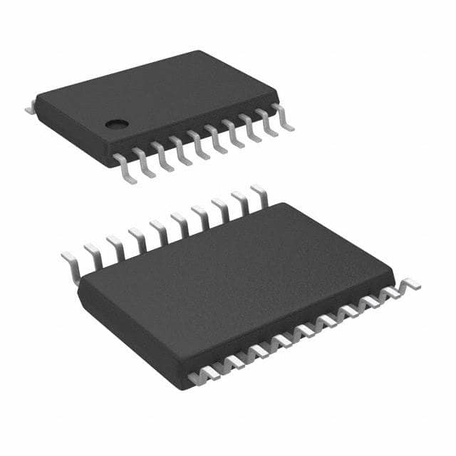
NLV74HC574ADTR2G
Product Overview
Category: Integrated Circuit (IC)
Use: The NLV74HC574ADTR2G is a high-speed octal D-type flip-flop with 3-state outputs. It is designed for general-purpose storage applications in digital systems.
Characteristics: - High-speed operation - 3-state outputs for bus-oriented applications - Wide operating voltage range - Low power consumption - Schmitt-trigger action on all inputs - Balanced propagation delays - Direct interface with TTL levels - Multiple package options available
Package: The NLV74HC574ADTR2G is available in a TSSOP-20 package, which stands for Thin Shrink Small Outline Package. This package offers a compact size and good thermal performance.
Essence: The essence of the NLV74HC574ADTR2G is its ability to store and manipulate digital information efficiently. It provides reliable and fast data storage capabilities for various digital systems.
Packaging/Quantity: The NLV74HC574ADTR2G is typically sold in reels containing 2500 units per reel.
Specifications
- Supply Voltage Range: 2 V to 6 V
- Input Voltage Range: -0.5 V to VCC + 0.5 V
- Output Voltage Range: -0.5 V to VCC + 0.5 V
- Operating Temperature Range: -40°C to +125°C
- Maximum Clock Frequency: 80 MHz
- Maximum Propagation Delay: 13 ns
Detailed Pin Configuration
The NLV74HC574ADTR2G has a total of 20 pins. The pin configuration is as follows:
- GND (Ground)
- Q0 (Output 0)
- D0 (Data input 0)
- D1 (Data input 1)
- D2 (Data input 2)
- D3 (Data input 3)
- D4 (Data input 4)
- D5 (Data input 5)
- D6 (Data input 6)
- D7 (Data input 7)
- Q7 (Output 7)
- OE (Output Enable)
- CP (Clock Pulse)
- MR (Master Reset)
- Q6 (Output 6)
- Q5 (Output 5)
- Q4 (Output 4)
- Q3 (Output 3)
- Q2 (Output 2)
- VCC (Supply Voltage)
Functional Features
The NLV74HC574ADTR2G offers the following functional features:
- Octal D-type flip-flop with 3-state outputs
- High-speed operation for efficient data storage and manipulation
- Schmitt-trigger action on all inputs for noise immunity
- Direct interface with TTL levels for easy integration into existing systems
- Balanced propagation delays for reliable timing
Advantages and Disadvantages
Advantages: - High-speed operation allows for fast data processing - 3-state outputs enable bus-oriented applications - Wide operating voltage range provides flexibility in various systems - Low power consumption helps conserve energy - Schmitt-trigger action on all inputs ensures noise immunity
Disadvantages: - Limited maximum clock frequency of 80 MHz - Propagation delay of up to 13 ns may affect real-time applications
Working Principles
The NLV74HC574ADTR2G operates based on the principles of digital storage using D-type flip-flops. It stores incoming data on its inputs and retains it until a clock pulse is received. The stored data is then available on the outputs. The 3-state outputs allow the device to be connected to a bus, enabling multiple devices to share the same data lines.
Detailed Application Field Plans
The NLV74HC574ADTR2G finds applications in various digital systems, including but not limited to: - Microcontrollers - Data storage systems - Communication equipment - Industrial automation - Automotive electronics
Detailed and Complete Alternative Models
Some alternative models that offer similar functionality to the NLV74HC574ADTR2G are: - SN74HC574N by Texas Instruments - MC74HC574AN by ON Semiconductor - CD74HC574E by Texas Instruments - 74HC574D by NXP Semiconductors - MM74HC574WMX by Fairchild Semiconductor
These alternative models can be considered based on specific requirements and availability in different regions.
Word count: 497 words
Senaraikan 10 soalan dan jawapan biasa yang berkaitan dengan aplikasi NLV74HC574ADTR2G dalam penyelesaian teknikal
Sure! Here are 10 common questions and answers related to the application of NLV74HC574ADTR2G in technical solutions:
Q: What is NLV74HC574ADTR2G? A: NLV74HC574ADTR2G is a high-speed CMOS octal D-type flip-flop with 3-state outputs, commonly used in digital logic applications.
Q: What is the operating voltage range for NLV74HC574ADTR2G? A: The operating voltage range for NLV74HC574ADTR2G is typically between 2V and 6V.
Q: What is the maximum clock frequency supported by NLV74HC574ADTR2G? A: NLV74HC574ADTR2G can support clock frequencies up to 74 MHz.
Q: How many flip-flops are there in NLV74HC574ADTR2G? A: NLV74HC574ADTR2G consists of 8 flip-flops, making it an octal (8-bit) device.
Q: What are the 3-state outputs in NLV74HC574ADTR2G used for? A: The 3-state outputs allow multiple devices to be connected together without causing conflicts or bus contention.
Q: Can NLV74HC574ADTR2G be used in both parallel and serial data transfer applications? A: Yes, NLV74HC574ADTR2G can be used in both parallel and serial data transfer applications, depending on the configuration.
Q: What is the typical propagation delay of NLV74HC574ADTR2G? A: The typical propagation delay of NLV74HC574ADTR2G is around 10 ns.
Q: Is NLV74HC574ADTR2G compatible with other logic families? A: Yes, NLV74HC574ADTR2G is compatible with a wide range of logic families, including TTL and CMOS.
Q: Can NLV74HC574ADTR2G be used in high-speed data communication applications? A: Yes, NLV74HC574ADTR2G is suitable for high-speed data communication applications due to its fast switching speed.
Q: What are some common applications of NLV74HC574ADTR2G? A: NLV74HC574ADTR2G is commonly used in microprocessors, memory interfaces, data storage systems, and general-purpose digital logic circuits.
I hope this helps! Let me know if you have any more questions.


