

NL17SV32XV5T2G
Basic Information Overview
- Category: Integrated Circuit (IC)
- Use: Logic Gate
- Characteristics: High-speed, Low-power consumption
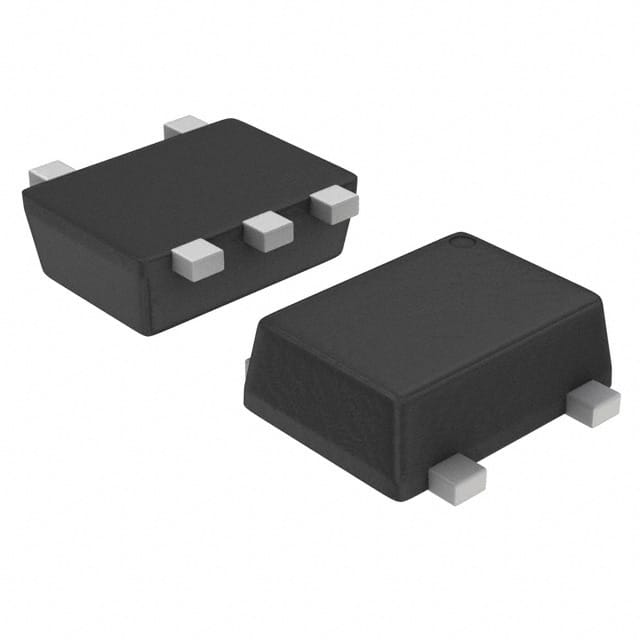
- Package: SOT-23-5
- Essence: Quad 2-input OR gate
- Packaging/Quantity: Tape and Reel, 3000 units per reel
Specifications
- Supply Voltage Range: 1.65V to 5.5V
- Input Voltage Range: -0.5V to VCC + 0.5V
- Output Voltage Range: 0V to VCC
- Operating Temperature Range: -40°C to +85°C
- Propagation Delay: 3.5ns (typical)
- Quiescent Current: 10μA (maximum)
Detailed Pin Configuration
The NL17SV32XV5T2G has a SOT-23-5 package with the following pin configuration:
____
   A --|    |
   B --|    |
   Y --|    |
   GND -|    |
   VCC -|____|
Functional Features
- Quad 2-input OR gate: The NL17SV32XV5T2G integrates four independent 2-input OR gates in a single package.
- High-speed operation: With a propagation delay of only 3.5ns, it enables fast signal processing.
- Low-power consumption: The IC operates at a low quiescent current of maximum 10μA, making it energy-efficient.
Advantages and Disadvantages
Advantages: - Compact design: The integration of four OR gates in one package saves board space. - Versatile: Suitable for various logic applications requiring OR gate functionality. - High-speed performance: Enables efficient signal processing in time-critical applications.
Disadvantages: - Limited input/output options: The IC only supports 2-input OR gates, which may not be suitable for complex logic operations. - Temperature limitations: The operating temperature range of -40°C to +85°C may restrict its use in extreme environments.
Working Principles
The NL17SV32XV5T2G operates based on the principles of digital logic. It performs the logical OR operation on two input signals (A and B) and provides the output signal (Y) based on the following truth table:
| A | B | Y |
|---|---|---|
| 0 | 0 | 0 |
| 0 | 1 | 1 |
| 1 | 0 | 1 |
| 1 | 1 | 1 |
The IC uses transistors and other electronic components to implement this logical function accurately and efficiently.
Detailed Application Field Plans
The NL17SV32XV5T2G is commonly used in various digital systems and applications, including: - Microcontrollers - Data communication devices - Industrial automation equipment - Consumer electronics - Automotive electronics
Its compact size, high-speed operation, and low-power consumption make it suitable for these applications where space, speed, and energy efficiency are crucial.
Detailed and Complete Alternative Models
Some alternative models that provide similar functionality to the NL17SV32XV5T2G include: - SN74LVC32A: Quad 2-input OR gate by Texas Instruments - MC14071B: Quad 2-input OR gate by ON Semiconductor - CD4071B: Quad 2-input OR gate by Texas Instruments
These alternatives offer comparable features and can be used as substitutes depending on specific requirements and availability.
Word count: 346 words
Senaraikan 10 soalan dan jawapan biasa yang berkaitan dengan aplikasi NL17SV32XV5T2G dalam penyelesaian teknikal
Sure! Here are 10 common questions and answers related to the application of NL17SV32XV5T2G in technical solutions:
Q: What is NL17SV32XV5T2G? A: NL17SV32XV5T2G is a specific model of a high-speed CMOS buffer IC (integrated circuit) used for signal conditioning and level shifting in various technical applications.
Q: What is the operating voltage range of NL17SV32XV5T2G? A: The operating voltage range of NL17SV32XV5T2G is typically between 1.65V and 3.6V.
Q: What is the maximum data rate supported by NL17SV32XV5T2G? A: NL17SV32XV5T2G supports a maximum data rate of up to 2.5 Gbps (gigabits per second).
Q: Can NL17SV32XV5T2G be used for level shifting between different voltage domains? A: Yes, NL17SV32XV5T2G can be used for level shifting between voltage domains, such as translating signals from 1.8V to 3.3V or vice versa.
Q: What is the typical propagation delay of NL17SV32XV5T2G? A: The typical propagation delay of NL17SV32XV5T2G is around 0.7 ns (nanoseconds).
Q: Is NL17SV32XV5T2G suitable for high-speed serial communication interfaces like USB or PCIe? A: Yes, NL17SV32XV5T2G is suitable for high-speed serial communication interfaces like USB or PCIe due to its high data rate capability.
Q: Can NL17SV32XV5T2G be used in battery-powered devices? A: Yes, NL17SV32XV5T2G can be used in battery-powered devices as it operates within a low voltage range and has low power consumption.
Q: Does NL17SV32XV5T2G have built-in ESD (electrostatic discharge) protection? A: Yes, NL17SV32XV5T2G typically includes built-in ESD protection to safeguard against electrostatic discharge events.
Q: What is the package type of NL17SV32XV5T2G? A: NL17SV32XV5T2G is commonly available in a small form factor package, such as a 16-pin TSSOP (Thin Shrink Small Outline Package).
Q: Are there any application notes or reference designs available for NL17SV32XV5T2G? A: Yes, the manufacturer of NL17SV32XV5T2G usually provides application notes and reference designs that can help with the implementation of this IC in various technical solutions.
Please note that the answers provided here are general and may vary depending on the specific datasheet and manufacturer's documentation for NL17SV32XV5T2G.