

NL17SG125P5T5G
Basic Information Overview
- Category: Integrated Circuit (IC)
- Use: Logic Gate
- Characteristics: Single Gate, Schmitt Trigger
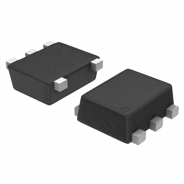
- Package: SOT-23-5
- Essence: High-Speed CMOS Technology
- Packaging/Quantity: Tape and Reel, 3000 pieces per reel
Specifications
- Supply Voltage Range: 1.65V to 5.5V
- Input Voltage Range: 0V to VCC
- Output Voltage Range: 0V to VCC
- Maximum Operating Frequency: 200MHz
- Propagation Delay: 3.5ns (typical)
- Input Capacitance: 3pF (typical)
- Output Current: ±8mA
Detailed Pin Configuration
The NL17SG125P5T5G has a total of 5 pins in the SOT-23 package. The pin configuration is as follows:
____
   1 -|    |- 5
   2 -|    |- 4
   3 -|____|- GND
Pin Description: 1. A: Input 2. Y: Output 3. NC: No Connection 4. GND: Ground 5. VCC: Power Supply
Functional Features
- Schmitt Trigger: Provides hysteresis to improve noise immunity and signal integrity.
- High-Speed Operation: Capable of operating at frequencies up to 200MHz.
- Wide Supply Voltage Range: Can be powered from 1.65V to 5.5V, making it suitable for various applications.
- Low Power Consumption: Consumes minimal power during operation.
Advantages and Disadvantages
Advantages: - Improved Noise Immunity: The Schmitt Trigger feature enhances the circuit's ability to reject noise. - Versatile Power Supply: The wide supply voltage range allows for flexibility in different power scenarios. - High-Speed Operation: Suitable for applications requiring fast signal processing.
Disadvantages: - Limited Number of Gates: Being a single gate IC, it can only perform a single logic function. - Small Package Size: The SOT-23 package may pose challenges in terms of handling and soldering for some users.
Working Principles
The NL17SG125P5T5G is based on high-speed CMOS technology. It utilizes a Schmitt Trigger circuit to provide hysteresis, which helps in reducing noise-induced errors and improving the stability of the output signal. The input signal is compared with predefined voltage thresholds, and the output changes state based on these thresholds.
Detailed Application Field Plans
The NL17SG125P5T5G can be used in various digital logic applications, including but not limited to: - Signal Conditioning: The Schmitt Trigger feature makes it suitable for cleaning up noisy signals before further processing. - Level Shifting: It can be used to shift logic levels between different voltage domains. - Oscillators: The high-speed operation enables its use in clock generation circuits. - Data Communication: Can be employed in serial data transmission systems for signal conditioning and level shifting.
Detailed and Complete Alternative Models
Some alternative models that offer similar functionality to the NL17SG125P5T5G include: - SN74LVC1G17DBVR (Texas Instruments) - MC74VHC1GT50DTT1G (ON Semiconductor) - 74LVC1G17GW (NXP Semiconductors)
These alternatives have comparable specifications and are available in similar packages, providing options for designers based on their specific requirements.
Word count: 399 words
Senaraikan 10 soalan dan jawapan biasa yang berkaitan dengan aplikasi NL17SG125P5T5G dalam penyelesaian teknikal
Sure! Here are 10 common questions and answers related to the application of NL17SG125P5T5G in technical solutions:
Q: What is NL17SG125P5T5G? A: NL17SG125P5T5G is a specific model of a logic gate, specifically a single-gate buffer, manufactured by ON Semiconductor.
Q: What is the purpose of NL17SG125P5T5G? A: The purpose of NL17SG125P5T5G is to provide signal buffering and level shifting capabilities in digital circuits.
Q: What voltage levels does NL17SG125P5T5G support? A: NL17SG125P5T5G supports a wide range of voltage levels, typically from 1.65V to 5.5V.
Q: Can NL17SG125P5T5G be used in both CMOS and TTL logic systems? A: Yes, NL17SG125P5T5G is compatible with both CMOS and TTL logic families, making it versatile for various applications.
Q: What is the maximum operating frequency of NL17SG125P5T5G? A: NL17SG125P5T5G has a high-speed operation capability, typically supporting frequencies up to several hundred megahertz (MHz).
Q: How many inputs and outputs does NL17SG125P5T5G have? A: NL17SG125P5T5G has one input and one output, as it is a single-gate buffer.
Q: Can NL17SG125P5T5G be used for voltage level translation between different logic families? A: Yes, NL17SG125P5T5G can be used for voltage level translation between different logic families, such as CMOS and TTL.
Q: What is the power supply range for NL17SG125P5T5G? A: NL17SG125P5T5G typically operates with a power supply voltage ranging from 1.65V to 5.5V.
Q: Is NL17SG125P5T5G available in surface mount packages? A: Yes, NL17SG125P5T5G is commonly available in surface mount packages, such as SOT-23 or SC-70.
Q: Can NL17SG125P5T5G be used in battery-powered applications? A: Yes, NL17SG125P5T5G's low power consumption makes it suitable for battery-powered applications where energy efficiency is crucial.
Please note that the answers provided here are general and may vary depending on specific datasheet specifications and application requirements.