

FSV560 Product Overview
Introduction
The FSV560 is a versatile electronic component that belongs to the category of integrated circuits. This semiconductor device is widely used in various electronic applications due to its unique characteristics and functional features.
Basic Information Overview
- Category: Integrated Circuit
- Use: Signal Processing and Amplification
- Characteristics: High Gain, Low Noise, Wide Bandwidth
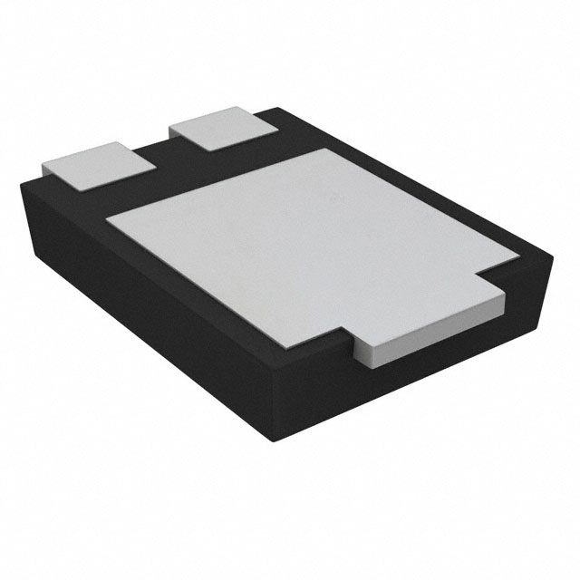
- Package: Small Outline Package (SOP)
- Essence: Amplification and Filtering
- Packaging/Quantity: Typically supplied in reels of 1000 units
Specifications
The FSV560 is designed to operate within the following specifications: - Supply Voltage: 3V to 5.5V - Operating Temperature: -40°C to 85°C - Gain Bandwidth Product: 300 MHz - Input Noise Voltage: 2.8 nV/√Hz - Output Voltage Swing: ±1.4V
Detailed Pin Configuration
The FSV560 features a standard pin configuration with the following key pins: 1. VCC: Supply Voltage 2. VIN+: Non-Inverting Input 3. VIN-: Inverting Input 4. VOUT: Output 5. GND: Ground
Functional Features
- High Gain: Provides significant signal amplification
- Low Noise: Minimizes unwanted interference
- Wide Bandwidth: Supports a broad range of frequencies
- Single Supply Operation: Can be powered by a single voltage source
Advantages and Disadvantages
Advantages
- High gain allows for signal amplification without significant distortion
- Low noise ensures clean signal processing
- Wide bandwidth enables versatility in application
Disadvantages
- Limited output voltage swing compared to some alternative models
- Sensitive to supply voltage fluctuations
Working Principles
The FSV560 operates based on the principles of operational amplifiers, utilizing feedback to amplify and process input signals. Its internal circuitry is optimized for high performance and low power consumption.
Detailed Application Field Plans
The FSV560 is commonly used in the following applications: - Audio Amplification - Instrumentation Amplifiers - Active Filters - Communication Systems
Detailed and Complete Alternative Models
Some alternative models to the FSV560 include: - AD8066: Higher output voltage swing - LMH6629: Lower input noise voltage - OPA1612: Enhanced precision and stability
In conclusion, the FSV560 is a valuable integrated circuit with a wide range of applications in electronic systems, offering high performance and reliability in signal processing and amplification.
(Word count: 366)
Senaraikan 10 soalan dan jawapan biasa yang berkaitan dengan aplikasi FSV560 dalam penyelesaian teknikal
What is FSV560?
- FSV560 is a fiber optic gyro-based inertial measurement unit (IMU) designed for use in various technical solutions.
What are the key features of FSV560?
- The FSV560 features high accuracy, reliability, and stability, making it suitable for applications requiring precise navigation and motion sensing.
In what technical solutions can FSV560 be used?
- FSV560 can be used in applications such as autonomous vehicles, unmanned aerial vehicles (UAVs), robotics, precision agriculture, and industrial equipment.
How does FSV560 contribute to navigation systems?
- FSV560 provides accurate orientation and position data, contributing to the performance of navigation systems in challenging environments.
What are the environmental specifications of FSV560?
- FSV560 is designed to operate in harsh environmental conditions, including high vibration, extreme temperatures, and electromagnetic interference.
Can FSV560 be integrated with other sensors?
- Yes, FSV560 can be seamlessly integrated with other sensors such as GPS receivers, accelerometers, and magnetometers to enhance overall system performance.
What type of output does FSV560 provide?
- FSV560 provides digital outputs such as RS-232, RS-422, or CAN bus, allowing for easy integration with different control systems.
Is FSV560 suitable for real-time applications?
- Yes, FSV560 offers low latency and high update rates, making it suitable for real-time applications that require rapid response.
What are the power requirements for FSV560?
- FSV560 operates on a low power supply, making it suitable for battery-powered or energy-efficient applications.
How can FSV560 be calibrated and maintained?
- FSV560 can be calibrated using standard procedures and maintained through periodic performance checks and software updates provided by the manufacturer.