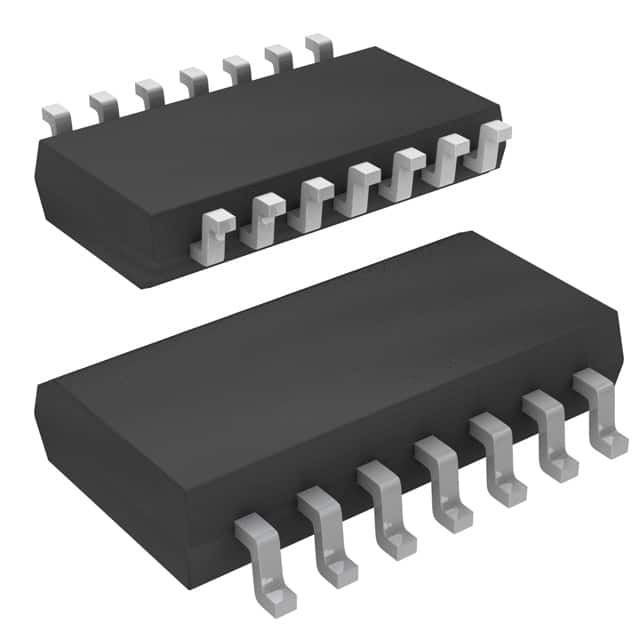
DM74ALS08SJ
Basic Information Overview
- Category: Integrated Circuit (IC)
- Use: Logic Gate
- Characteristics: Quad 2-Input AND Gate
- Package: 14-Pin Small Outline Integrated Circuit (SOIC)
- Essence: High-speed, low-power consumption logic gate
- Packaging/Quantity: Available in reels of 2500 units
Specifications
- Supply Voltage Range: 4.75V to 5.25V
- Input Voltage Range: 0V to VCC
- Output Voltage Range: 0V to VCC
- Operating Temperature Range: -40°C to +85°C
- Propagation Delay Time: 9ns (typical)
- Power Dissipation: 22mW (typical)
Detailed Pin Configuration
- A1: Input A1
- B1: Input B1
- Y1: Output Y1
- A2: Input A2
- B2: Input B2
- Y2: Output Y2
- GND: Ground
- Y3: Output Y3
- B3: Input B3
- A3: Input A3
- Y4: Output Y4
- B4: Input B4
- A4: Input A4
- VCC: Positive Supply Voltage
Functional Features
- Performs logical AND operation on two input signals
- Provides four independent AND gates in a single package
- High-speed operation allows for quick signal processing
- Low power consumption makes it suitable for battery-powered devices
- Wide operating temperature range enables usage in various environments
Advantages and Disadvantages
Advantages
- Compact design with multiple gates in a single package saves board space
- High-speed operation enhances overall system performance
- Low power consumption prolongs battery life in portable devices
Disadvantages
- Limited number of inputs and outputs per gate
- Not suitable for applications requiring complex logic operations
Working Principles
The DM74ALS08SJ is a quad 2-input AND gate that performs the logical AND operation on two input signals. It consists of four independent AND gates, each with two inputs and one output. The gate operates by comparing the input signals and producing an output signal only when both inputs are high (logic level 1). Otherwise, the output remains low (logic level 0).
Detailed Application Field Plans
The DM74ALS08SJ is commonly used in digital systems where logical AND operations are required. Some typical application fields include: - Data processing units - Arithmetic circuits - Control systems - Communication devices - Industrial automation
Detailed and Complete Alternative Models
- SN74LS08: Quad 2-Input AND Gate by Texas Instruments
- MC74HC08: Quad 2-Input AND Gate by ON Semiconductor
- CD4081: Quad 2-Input AND Gate by Texas Instruments
- 74HCT08: Quad 2-Input AND Gate by NXP Semiconductors
- 74F08: Quad 2-Input AND Gate by Fairchild Semiconductor
(Note: This list is not exhaustive and there are several other alternative models available in the market.)
In conclusion, the DM74ALS08SJ is a quad 2-input AND gate integrated circuit that offers high-speed operation, low power consumption, and compact design. It finds applications in various digital systems and can be replaced by alternative models depending on specific requirements.
Senaraikan 10 soalan dan jawapan biasa yang berkaitan dengan aplikasi DM74ALS08SJ dalam penyelesaian teknikal
Sure! Here are 10 common questions and answers related to the application of DM74ALS08SJ in technical solutions:
Q: What is DM74ALS08SJ? A: DM74ALS08SJ is a quad 2-input AND gate integrated circuit (IC) that can be used in various digital logic applications.
Q: What is the operating voltage range for DM74ALS08SJ? A: The operating voltage range for DM74ALS08SJ is typically between 4.5V and 5.5V.
Q: How many AND gates are there in DM74ALS08SJ? A: DM74ALS08SJ contains four independent AND gates, each with two inputs and one output.
Q: What is the maximum input current for DM74ALS08SJ? A: The maximum input current for DM74ALS08SJ is typically 0.4mA.
Q: Can DM74ALS08SJ be used in high-speed applications? A: Yes, DM74ALS08SJ is designed for high-speed operation and can be used in applications requiring fast switching times.
Q: What is the propagation delay of DM74ALS08SJ? A: The propagation delay of DM74ALS08SJ is typically around 9 nanoseconds.
Q: Is DM74ALS08SJ compatible with TTL logic levels? A: Yes, DM74ALS08SJ is compatible with both TTL and CMOS logic levels, making it versatile for different system designs.
Q: Can DM74ALS08SJ drive capacitive loads directly? A: No, DM74ALS08SJ is not recommended for driving capacitive loads directly. It is advisable to use a buffer or driver IC for such applications.
Q: What is the power dissipation of DM74ALS08SJ? A: The power dissipation of DM74ALS08SJ is typically around 22mW.
Q: Can DM74ALS08SJ be used in automotive applications? A: Yes, DM74ALS08SJ is suitable for automotive applications as it can operate within the specified temperature range and withstand voltage fluctuations.
Please note that these answers are general and may vary depending on specific datasheet specifications and application requirements.


