

74LVQ240QSC
Product Overview
- Category: Integrated Circuit (IC)
- Use: Logic Gate
- Characteristics: Low-voltage, Quad Buffer/Line Driver with 3-State Outputs
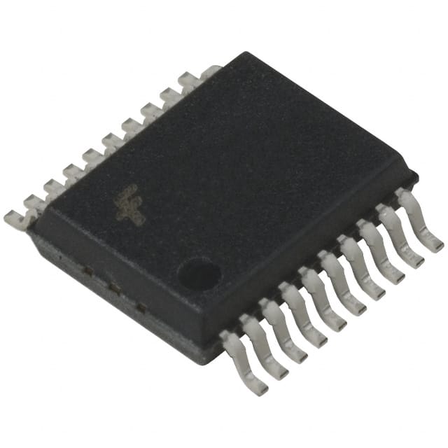
- Package: QSOP (Quarter Small Outline Package)
- Essence: Buffer and line driver for digital signal transmission
- Packaging/Quantity: Available in reels of 2500 units
Specifications
- Supply Voltage Range: 1.65V to 5.5V
- High-Level Input Voltage: 2V to VCC + 0.5V
- Low-Level Input Voltage: -0.5V to 0.8V
- High-Level Output Voltage: VCC - 0.5V
- Low-Level Output Voltage: 0.5V
- Maximum Operating Frequency: 200MHz
- Propagation Delay Time: 4.6ns (typical)
Detailed Pin Configuration
The 74LVQ240QSC has a total of 20 pins, which are assigned as follows:
- A1 - Input A1
- Y1 - Output Y1
- A2 - Input A2
- Y2 - Output Y2
- GND - Ground
- A3 - Input A3
- Y3 - Output Y3
- A4 - Input A4
- Y4 - Output Y4
- OE - Output Enable
- GND - Ground
- Y5 - Output Y5
- A5 - Input A5
- Y6 - Output Y6
- A6 - Input A6
- Y7 - Output Y7
- VCC - Power Supply
- A7 - Input A7
- Y8 - Output Y8
- A8 - Input A8
Functional Features
- Quad buffer/line driver with 3-state outputs
- Non-inverting logic gates
- High-speed operation
- Low power consumption
- Wide supply voltage range
- 3-state outputs for bus-oriented applications
Advantages and Disadvantages
Advantages: - High-speed operation allows for efficient signal transmission - Wide supply voltage range enables compatibility with various systems - Low power consumption reduces energy usage - 3-state outputs facilitate bus-oriented applications
Disadvantages: - Limited number of inputs and outputs (8 each) - Not suitable for high-voltage applications
Working Principles
The 74LVQ240QSC is a quad buffer/line driver that operates as a non-inverting logic gate. It accepts digital input signals and provides amplified output signals. The device features 3-state outputs, which allow multiple drivers to share a common bus without interference. The buffer/line driver operates within a specified supply voltage range and provides fast propagation delay times for efficient signal transmission.
Detailed Application Field Plans
The 74LVQ240QSC is commonly used in various digital systems and applications, including:
- Microcontrollers and microprocessors
- Data communication systems
- Industrial automation
- Automotive electronics
- Consumer electronics
- Robotics
- Instrumentation and measurement equipment
Detailed and Complete Alternative Models
Some alternative models that can be considered as replacements for the 74LVQ240QSC are:
- SN74LVC240A - Low-Voltage Octal Buffer/Line Driver with 3-State Outputs
- MC74VHC240 - Octal Bus Buffer/Line Driver with 3-State Outputs
- CD74HCT240 - Octal Buffer/Line Driver with 3-State Outputs
- TC7WZ240FK - Low-Voltage Octal Buffer/Line Driver with 3-State Outputs
These alternative models offer similar functionality and characteristics, providing options for different design requirements.
In conclusion, the 74LVQ240QSC is a versatile integrated circuit that serves as a quad buffer/line driver for digital signal transmission. Its high-speed operation, low power consumption, and wide supply voltage range make it suitable for various applications in different fields.
Senaraikan 10 soalan dan jawapan biasa yang berkaitan dengan aplikasi 74LVQ240QSC dalam penyelesaian teknikal
Sure! Here are 10 common questions and answers related to the application of 74LVQ240QSC in technical solutions:
Question: What is the 74LVQ240QSC?
- Answer: The 74LVQ240QSC is a type of octal buffer/line driver integrated circuit (IC) that can be used in various digital logic applications.Question: What is the voltage supply range for the 74LVQ240QSC?
- Answer: The voltage supply range for this IC is typically between 1.65V and 5.5V.Question: How many input/output pins does the 74LVQ240QSC have?
- Answer: This IC has 8 input pins and 8 output pins, making it suitable for octal buffer applications.Question: Can the 74LVQ240QSC handle bidirectional data flow?
- Answer: Yes, this IC supports bidirectional data flow, allowing data to be transmitted in both directions.Question: What is the maximum operating frequency of the 74LVQ240QSC?
- Answer: The maximum operating frequency of this IC is typically around 200 MHz, making it suitable for high-speed applications.Question: Does the 74LVQ240QSC have any built-in protection features?
- Answer: Yes, this IC includes built-in ESD protection on its inputs and outputs, helping to safeguard against electrostatic discharge.Question: Can the 74LVQ240QSC be used in mixed-voltage systems?
- Answer: Yes, this IC is designed to be compatible with mixed-voltage systems, allowing for easy integration into different types of circuits.Question: What is the power consumption of the 74LVQ240QSC?
- Answer: The power consumption of this IC is relatively low, making it suitable for battery-powered or energy-efficient applications.Question: Can the 74LVQ240QSC drive capacitive loads?
- Answer: Yes, this IC has a high output drive capability and can drive capacitive loads without requiring additional external components.Question: Are there any recommended application circuits available for the 74LVQ240QSC?
- Answer: Yes, the datasheet for this IC typically includes recommended application circuits and example schematics that can be used as a starting point for designing with the 74LVQ240QSC.
Please note that these answers are general and may vary depending on specific datasheets and manufacturer specifications.