

Encyclopedia Entry: 74ACT899QC
Product Information Overview
- Category: Integrated Circuit (IC)
- Use: Logic Function
- Characteristics: High-Speed, Low-Power, 8-Bit Universal Shift/Storage Register
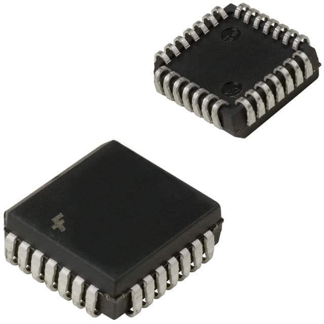
- Package: Quad Flat Package (QFP)
- Essence: The 74ACT899QC is a versatile integrated circuit that combines the functionality of an 8-bit universal shift register and storage register. It is designed to operate at high speeds while consuming low power.
- Packaging/Quantity: The 74ACT899QC is typically packaged in a Quad Flat Package (QFP) and is available in various quantities.
Specifications
The 74ACT899QC has the following specifications:
- Operating Voltage Range: 4.5V to 5.5V
- Input Voltage Range: 0V to VCC
- Output Voltage Range: 0V to VCC
- Operating Temperature Range: -40°C to +85°C
- Propagation Delay: 6ns (typical)
- Power Dissipation: 500mW (max)
Detailed Pin Configuration
The 74ACT899QC has a total of 20 pins. The pin configuration is as follows:
- SRCLK (Shift Register Clock Input)
- RCLK (Storage Register Clock Input)
- SER (Serial Data Input)
- SCLR (Shift/Storage Register Clear Input)
- QA-QH (Parallel Outputs)
- GND (Ground)
- QH' (Serial Output)
- VCC (Positive Power Supply)
Functional Features
The 74ACT899QC offers the following functional features:
- Universal Shift Register: Allows data to be shifted in either direction (left or right).
- Storage Register: Can store the data present at the parallel inputs.
- High-Speed Operation: Designed to operate at high clock frequencies, making it suitable for applications requiring fast data processing.
- Low Power Consumption: The IC is designed to minimize power consumption, making it energy-efficient.
Advantages and Disadvantages
Advantages of the 74ACT899QC include:
- Versatility: Combines the functionality of a shift register and storage register in a single IC.
- High-Speed Operation: Suitable for applications that require fast data processing.
- Low Power Consumption: Energy-efficient design.
Disadvantages of the 74ACT899QC include:
- Limited Input/Output Options: The IC has a fixed number of input and output pins, which may restrict its use in certain applications.
- Temperature Sensitivity: The operating temperature range is limited to -40°C to +85°C, which may not be suitable for extreme environments.
Working Principles
The 74ACT899QC operates based on the principles of digital logic. It utilizes clock signals to control the shifting and storage of data. When the appropriate clock signals are applied, the IC can shift data in either direction or store the data present at the parallel inputs. This allows for flexible data manipulation and processing.
Detailed Application Field Plans
The 74ACT899QC can be used in various applications, including:
- Data Communication Systems
- Digital Signal Processing
- Microcontroller Interfacing
- Industrial Automation
- Consumer Electronics
Detailed and Complete Alternative Models
Some alternative models to the 74ACT899QC include:
- 74HC595: 8-Bit Shift Register with Output Latches
- CD4021B: 8-Stage Static Shift Register
- SN74LS164N: 8-Bit Serial-In/Parallel-Out Shift Register
- MC74HC165A: 8-Bit Parallel-Load Shift Register
- CD4094BE: 8-Stage Shift-and-Store Bus Register
These alternative models offer similar functionality and can be used as substitutes for the 74ACT899QC in various applications.
Word count: 410 words
Senaraikan 10 soalan dan jawapan biasa yang berkaitan dengan aplikasi 74ACT899QC dalam penyelesaian teknikal
Sure! Here are 10 common questions and answers related to the application of 74ACT899QC in technical solutions:
Q: What is the 74ACT899QC? A: The 74ACT899QC is a high-speed, 8-bit universal shift/storage register with three-state outputs.
Q: What are the key features of the 74ACT899QC? A: The key features include parallel-to-serial or serial-to-parallel data conversion, three-state outputs, and high-speed operation.
Q: How can I use the 74ACT899QC for parallel-to-serial data conversion? A: Connect the parallel data inputs (D0-D7) to your parallel data source, and use the shift clock (SHCP) and storage clock (STCP) signals to control the conversion process.
Q: Can the 74ACT899QC be used for serial-to-parallel data conversion as well? A: Yes, by connecting the serial data input (DS) to your serial data source and using the shift clock (SHCP) and storage clock (STCP) signals appropriately.
Q: What is the maximum operating frequency of the 74ACT899QC? A: The 74ACT899QC can operate at frequencies up to 100 MHz.
Q: Can I cascade multiple 74ACT899QC devices together? A: Yes, you can cascade multiple devices to increase the number of bits in the shift register.
Q: How do I enable or disable the three-state outputs of the 74ACT899QC? A: Use the output enable (OE) signal to enable or disable the three-state outputs.
Q: What is the power supply voltage range for the 74ACT899QC? A: The 74ACT899QC operates with a power supply voltage range of 4.5V to 5.5V.
Q: Can the 74ACT899QC be used in both TTL and CMOS logic systems? A: Yes, the 74ACT899QC is compatible with both TTL and CMOS logic levels.
Q: Are there any specific application notes or reference designs available for the 74ACT899QC? A: Yes, you can refer to the datasheet provided by the manufacturer for detailed application notes and reference designs.
Please note that these answers are general and may vary depending on the specific requirements and implementation of your technical solution.