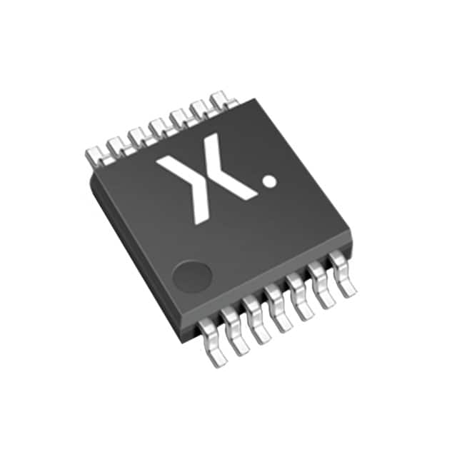
74HC30PW,118
Basic Information Overview
- Category: Integrated Circuit (IC)
- Use: Logic Gate
- Characteristics: High-speed operation, low power consumption
- Package: TSSOP (Thin Shrink Small Outline Package)
- Essence: 8-input NAND gate
- Packaging/Quantity: Tape and reel, 2500 units per reel
Specifications
- Supply Voltage Range: 2.0V to 6.0V
- Input Voltage Range: -0.5V to VCC + 0.5V
- Output Voltage Range: -0.5V to VCC + 0.5V
- Operating Temperature Range: -40°C to +125°C
- Propagation Delay: 9 ns (typical)
Detailed Pin Configuration
The 74HC30PW,118 has a total of 14 pins: 1. Pin 1: A1 (Input A1) 2. Pin 2: B1 (Input B1) 3. Pin 3: C1 (Input C1) 4. Pin 4: D1 (Input D1) 5. Pin 5: E1 (Input E1) 6. Pin 6: F1 (Input F1) 7. Pin 7: G1 (Input G1) 8. Pin 8: H1 (Input H1) 9. Pin 9: GND (Ground) 10. Pin 10: Y1 (Output Y1) 11. Pin 11: Y2 (Output Y2) 12. Pin 12: Y3 (Output Y3) 13. Pin 13: Y4 (Output Y4) 14. Pin 14: VCC (Supply Voltage)
Functional Features
- The 74HC30PW,118 is an 8-input NAND gate that performs the logical NAND operation on its inputs.
- It provides a high-speed and low-power solution for digital logic applications.
- The device operates within a wide supply voltage range, making it suitable for various electronic systems.
Advantages and Disadvantages
Advantages: - High-speed operation allows for efficient processing of logic operations. - Low power consumption helps in reducing overall system power requirements. - Wide supply voltage range enables compatibility with different voltage levels.
Disadvantages: - Limited number of inputs (8) may restrict the complexity of logic functions that can be implemented. - TSSOP package may require careful handling during assembly to avoid damage.
Working Principles
The 74HC30PW,118 is based on CMOS (Complementary Metal-Oxide-Semiconductor) technology. It utilizes multiple transistors to implement the NAND gate functionality. When all input signals are low, the output is high. If any of the inputs are high, the output becomes low.
Detailed Application Field Plans
The 74HC30PW,118 can be used in various digital logic applications, including but not limited to: - Arithmetic circuits - Data processing systems - Control systems - Communication devices
Detailed and Complete Alternative Models
Some alternative models to the 74HC30PW,118 include: - 74LS30: A TTL (Transistor-Transistor Logic) version of the 8-input NAND gate. - CD4081: A CMOS quad 2-input AND gate. - SN54HC30: A high-speed CMOS 8-input NAND gate.
These alternatives offer similar functionality but may have differences in terms of speed, power consumption, and voltage compatibility.
In conclusion, the 74HC30PW,118 is an integrated circuit belonging to the logic gate category. It is an 8-input NAND gate with high-speed operation and low power consumption. The IC comes in a TSSOP package and operates within a wide supply voltage range. It finds applications in various digital logic systems and has alternative models with similar functionality.
Senaraikan 10 soalan dan jawapan biasa yang berkaitan dengan aplikasi 74HC30PW,118 dalam penyelesaian teknikal
Sure! Here are 10 common questions and answers related to the application of 74HC30PW,118 in technical solutions:
Q: What is the 74HC30PW,118? A: The 74HC30PW,118 is a 8-input NAND gate IC (integrated circuit) that can be used in various digital logic applications.
Q: What is the operating voltage range for the 74HC30PW,118? A: The operating voltage range for the 74HC30PW,118 is typically between 2V and 6V.
Q: How many inputs does the 74HC30PW,118 have? A: The 74HC30PW,118 has 8 inputs, allowing you to connect multiple signals for logical operations.
Q: What is the maximum output current of the 74HC30PW,118? A: The maximum output current of the 74HC30PW,118 is around 5.2mA.
Q: Can the 74HC30PW,118 be used for level shifting? A: Yes, the 74HC30PW,118 can be used for level shifting as it operates at different voltage levels.
Q: What is the propagation delay of the 74HC30PW,118? A: The propagation delay of the 74HC30PW,118 is typically around 11ns.
Q: Can I use the 74HC30PW,118 in high-speed applications? A: Yes, the 74HC30PW,118 is suitable for high-speed applications due to its low propagation delay.
Q: Is the 74HC30PW,118 compatible with TTL (Transistor-Transistor Logic) inputs? A: Yes, the 74HC30PW,118 is compatible with TTL inputs, making it versatile for interfacing with different logic families.
Q: Can I use the 74HC30PW,118 in both commercial and industrial applications? A: Yes, the 74HC30PW,118 is designed to meet the requirements of both commercial and industrial applications.
Q: Are there any specific precautions to consider when using the 74HC30PW,118? A: It is important to ensure that the power supply voltage does not exceed the specified range and to avoid static discharge during handling to prevent damage to the IC.
Please note that these answers are general and may vary depending on the specific datasheet and manufacturer's recommendations for the 74HC30PW,118.


