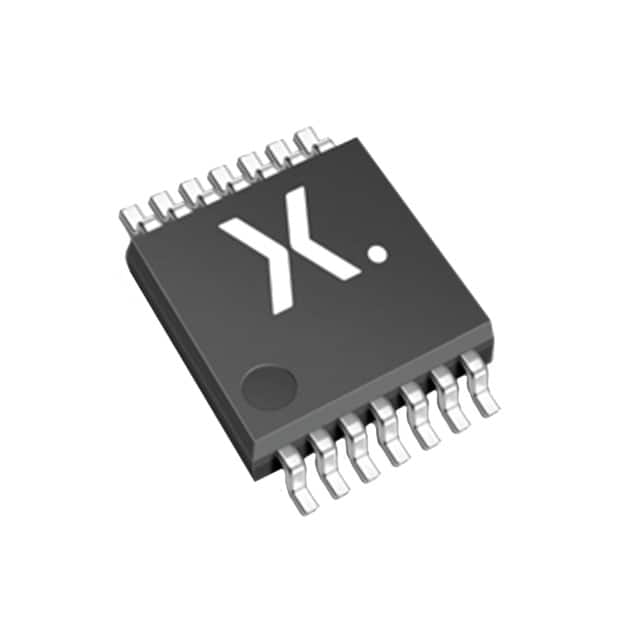
Encyclopedia Entry: 74ALVC00PW,118
Product Overview
Category
The 74ALVC00PW,118 belongs to the category of integrated circuits (ICs), specifically digital logic gates.
Use
This product is commonly used in electronic devices and systems for logical operations. It serves as a quad 2-input NAND gate, providing essential functionality for various applications.
Characteristics
- High-speed operation: The 74ALVC00PW,118 offers fast switching times, enabling efficient data processing.
- Low power consumption: This IC is designed to minimize power usage, making it suitable for battery-powered devices.
- Wide supply voltage range: It can operate within a broad range of supply voltages, enhancing its versatility.
- Compatibility: The 74ALVC00PW,118 is compatible with both TTL and CMOS logic levels, facilitating integration into different systems.
Package and Quantity
The 74ALVC00PW,118 is available in a small-sized TSSOP-14 package. Each package contains one unit of the IC.
Specifications
- Supply Voltage Range: 1.65V to 3.6V
- Input Voltage Range: -0.5V to VCC + 0.5V
- Output Voltage Range: -0.5V to VCC + 0.5V
- Operating Temperature Range: -40°C to +85°C
- Propagation Delay Time: 2.8ns (typical) at 3.3V supply voltage
Pin Configuration
The 74ALVC00PW,118 has a total of 14 pins, arranged as follows:
+---+--+---+
   A1 -|1  +--+ 14|- VCC
   B1 -|2         |- A2
   Y1 -|3         |- B2
  GND -|4         |- Y2
   A3 -|5         |- B3
   B3 -|6         |- Y3
   Y3 -|7         |- GND
   A4 -|8         |- B4
   B4 -|9         |- Y4
   Y4 -|10        |- GND
  GND -|11        |- GND
  GND -|12        |- GND
  GND -|13        |- GND
  GND -|14        |- GND
       +----------+
Functional Features
The 74ALVC00PW,118 is a quad 2-input NAND gate. It performs the logical operation of NAND on two input signals (A and B) and provides the resulting output signal (Y). The IC operates with high speed and low power consumption, making it suitable for various digital applications.
Advantages and Disadvantages
Advantages
- High-speed operation enables efficient data processing.
- Low power consumption makes it suitable for battery-powered devices.
- Wide supply voltage range enhances versatility.
- Compatibility with TTL and CMOS logic levels facilitates integration into different systems.
Disadvantages
- Limited number of inputs and outputs restricts complex logic operations.
- Small package size may require additional precautions during handling and soldering.
Working Principles
The 74ALVC00PW,118 operates based on the principles of semiconductor logic gates. In the case of a NAND gate, the output is low only when both inputs are high. Otherwise, the output remains high. This behavior allows for logical operations such as AND and NOT.
Application Field Plans
The 74ALVC00PW,118 finds application in various electronic systems, including but not limited to: 1. Microcontrollers and microprocessors 2. Communication devices 3. Data storage systems 4. Industrial automation equipment 5. Automotive electronics
Alternative Models
Several alternative models with similar functionality to the 74ALVC00PW,118 include: - SN74LVC00APW - MC74VHC00DTG - CD74HCT00M96
These alternatives can be considered based on specific requirements and availability.
In conclusion, the 74ALVC00PW,118 is a versatile quad 2-input NAND gate IC that offers high-speed operation, low power consumption, and compatibility with different logic levels. Its compact package and wide range of applications make it a valuable component in various electronic systems.
Word Count: 511
Senaraikan 10 soalan dan jawapan biasa yang berkaitan dengan aplikasi 74ALVC00PW,118 dalam penyelesaian teknikal
Sure! Here are 10 common questions and answers related to the application of 74ALVC00PW,118 in technical solutions:
Q: What is the function of the 74ALVC00PW,118? A: The 74ALVC00PW,118 is a quad 2-input NAND gate integrated circuit (IC) that performs logical NAND operations.
Q: What is the operating voltage range for the 74ALVC00PW,118? A: The 74ALVC00PW,118 operates within a voltage range of 1.65V to 3.6V.
Q: Can the 74ALVC00PW,118 be used in both digital and analog applications? A: No, the 74ALVC00PW,118 is primarily designed for digital applications and is not recommended for analog use.
Q: What is the maximum output current of the 74ALVC00PW,118? A: The maximum output current of the 74ALVC00PW,118 is typically around 24mA.
Q: Is the 74ALVC00PW,118 compatible with other logic families? A: Yes, the 74ALVC00PW,118 is compatible with various logic families such as TTL, CMOS, and LVTTL.
Q: Can I connect the outputs of multiple 74ALVC00PW,118 ICs together? A: Yes, you can connect the outputs of multiple 74ALVC00PW,118 ICs together to create larger logic functions.
Q: What is the propagation delay of the 74ALVC00PW,118? A: The propagation delay of the 74ALVC00PW,118 is typically around 2.5ns.
Q: Can the 74ALVC00PW,118 be used in high-speed applications? A: Yes, the 74ALVC00PW,118 is designed for high-speed operation and can be used in such applications.
Q: Does the 74ALVC00PW,118 have built-in protection against electrostatic discharge (ESD)? A: Yes, the 74ALVC00PW,118 has built-in ESD protection to safeguard against damage during handling and operation.
Q: What package options are available for the 74ALVC00PW,118? A: The 74ALVC00PW,118 is available in various package options, including TSSOP, SOIC, and VFBGA.
Please note that these answers are general and may vary depending on the specific datasheet and manufacturer's specifications of the 74ALVC00PW,118 IC.


