

MAP5KE100CAE3
Introduction
The MAP5KE100CAE3 is a high-performance transient voltage suppressor (TVS) diode designed to protect sensitive electronic equipment from voltage transients induced by lightning and other transient voltage events. This entry provides an overview of the product, including its basic information, specifications, detailed pin configuration, functional features, advantages and disadvantages, working principles, application field plans, and alternative models.
Basic Information Overview
- Category: TVS Diode
- Use: Protection against voltage transients
- Characteristics: High performance, fast response time, low clamping voltage
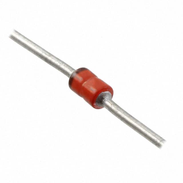
- Package: SMC (DO-214AB)
- Essence: Safeguarding sensitive electronic equipment
- Packaging/Quantity: Tape & Reel, 3000 units per reel
Specifications
- Peak Pulse Power: 5000W
- Standoff Voltage: 85V
- Breakdown Voltage: 94.4V to 105V
- Operating Temperature Range: -55°C to +150°C
- RoHS Compliant: Yes
Detailed Pin Configuration
The MAP5KE100CAE3 TVS diode has a standard SMC (DO-214AB) package with two leads. The pin configuration is as follows: - Pin 1: Anode - Pin 2: Cathode
Functional Features
- Fast response time
- Low clamping voltage
- High surge capability
- RoHS compliant
Advantages and Disadvantages
Advantages
- Excellent protection against transient voltage events
- Fast response time ensures minimal impact on protected circuits
- RoHS compliance for environmental sustainability
Disadvantages
- Higher cost compared to standard diodes
- Slight leakage current in normal operation
Working Principles
The MAP5KE100CAE3 operates based on the principle of avalanche breakdown. When a transient voltage event occurs, the TVS diode rapidly conducts, diverting excess current away from the protected circuit and clamping the voltage to a safe level.
Detailed Application Field Plans
The MAP5KE100CAE3 is widely used in various applications requiring protection against voltage transients, including: - Power supplies - Communication systems - Industrial control systems - Automotive electronics - Consumer electronics
Detailed and Complete Alternative Models
- Alternative Model 1: P6KE100CA
- Standoff Voltage: 85V
- Breakdown Voltage: 95V to 106V
- Package: DO-15
- Alternative Model 2: SMAJ100A
- Standoff Voltage: 85V
- Breakdown Voltage: 94.4V to 105V
- Package: SMA (DO-214AC)
In conclusion, the MAP5KE100CAE3 TVS diode offers robust protection against transient voltage events, making it an essential component in safeguarding sensitive electronic equipment across various industries.
Word Count: 443
Senaraikan 10 soalan dan jawapan biasa yang berkaitan dengan aplikasi MAP5KE100CAE3 dalam penyelesaian teknikal
What is the maximum voltage rating of MAP5KE100CAE3?
- The maximum voltage rating of MAP5KE100CAE3 is 100V.
What is the peak pulse power of MAP5KE100CAE3?
- The peak pulse power of MAP5KE100CAE3 is 5000W.
What is the typical clamping voltage of MAP5KE100CAE3?
- The typical clamping voltage of MAP5KE100CAE3 is 162V at 10A.
What are the applications of MAP5KE100CAE3?
- MAP5KE100CAE3 is commonly used in surge protection for sensitive electronics, such as in telecommunications equipment, industrial control systems, and automotive electronics.
What is the response time of MAP5KE100CAE3?
- The response time of MAP5KE100CAE3 is typically less than 1 picosecond.
What is the operating temperature range of MAP5KE100CAE3?
- MAP5KE100CAE3 has an operating temperature range of -55°C to 175°C.
Does MAP5KE100CAE3 meet industry standards for surge protection?
- Yes, MAP5KE100CAE3 complies with industry standards such as IEC 61000-4-5 for surge protection devices.
Can MAP5KE100CAE3 be used in high-speed data transmission applications?
- Yes, MAP5KE100CAE3 is suitable for use in high-speed data transmission applications due to its fast response time and low clamping voltage.
What packaging options are available for MAP5KE100CAE3?
- MAP5KE100CAE3 is available in various packaging options, including DO-201, DO-15, and SMC packages.
Is MAP5KE100CAE3 RoHS compliant?
- Yes, MAP5KE100CAE3 is RoHS compliant, making it suitable for use in environmentally conscious designs.