

AT49BV040-12JC
Product Overview
Category
AT49BV040-12JC belongs to the category of non-volatile memory devices.
Use
It is primarily used for storing data in electronic systems, such as microcontrollers and embedded systems.
Characteristics
- Non-volatile: Retains data even when power is turned off.
- High storage capacity: The AT49BV040-12JC has a storage capacity of 4 megabits (512 kilobytes).
- Fast access time: It has a fast access time of 120 nanoseconds.
- Low power consumption: The device operates on low power, making it suitable for battery-powered applications.
Package
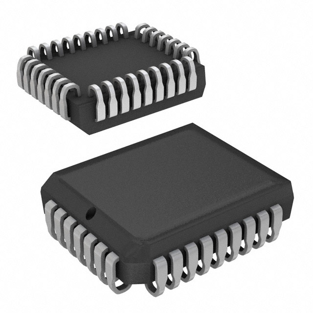
The AT49BV040-12JC is available in a 32-pin PLCC (Plastic Leaded Chip Carrier) package.
Essence
The essence of AT49BV040-12JC lies in its ability to provide reliable and non-volatile storage for electronic systems.
Packaging/Quantity
The device is typically packaged in reels or tubes, with quantities varying based on customer requirements.
Specifications
- Memory Type: Flash
- Organization: 512K x 8 bits
- Voltage Range: 2.7V - 3.6V
- Access Time: 120 ns
- Operating Temperature Range: -40°C to +85°C
- Erase/Program Cycle Endurance: 10,000 cycles
Detailed Pin Configuration
The AT49BV040-12JC has a total of 32 pins. Here is the detailed pin configuration:
- A0 - Address Input
- A1 - Address Input
- A2 - Address Input
- A3 - Address Input
- A4 - Address Input
- A5 - Address Input
- A6 - Address Input
- A7 - Address Input
- A8 - Address Input
- A9 - Address Input
- A10 - Address Input
- A11 - Address Input
- A12 - Address Input
- A13 - Address Input
- A14 - Address Input
- A15 - Address Input
- CE# - Chip Enable Input
- OE# - Output Enable Input
- WE# - Write Enable Input
- RESET# - Reset Input
- BYTE# - Byte/Word Organization Select Input
- VCC - Power Supply
- DQ0 - Data Input/Output
- DQ1 - Data Input/Output
- DQ2 - Data Input/Output
- DQ3 - Data Input/Output
- DQ4 - Data Input/Output
- DQ5 - Data Input/Output
- DQ6 - Data Input/Output
- DQ7 - Data Input/Output
- GND - Ground
- NC - No Connection
Functional Features
- High-speed data transfer: The AT49BV040-12JC supports fast data transfer rates, allowing for efficient read and write operations.
- Sector erase capability: It provides the ability to erase specific sectors of the memory, enabling selective data modification.
- Built-in protection mechanisms: The device incorporates various protection features, such as program and erase lockout, to prevent accidental data corruption.
Advantages and Disadvantages
Advantages
- Non-volatile storage: Data is retained even without power, ensuring data integrity.
- High storage capacity: The 4 megabit capacity allows for ample data storage.
- Fast access time: The device offers quick access to stored data.
- Low power consumption: It operates on low power, making it suitable for battery-powered applications.
Disadvantages
- Limited erase/write cycles: The AT49BV040-12JC has a limited endurance of 10,000 erase/write cycles.
- Relatively small storage capacity: Compared to other memory devices, the 4 megabit capacity may be insufficient for certain applications.
Working Principles
The AT49BV040-12JC utilizes flash memory technology to store and retrieve data. It employs a combination of floating-gate transistors and charge storage mechanisms to retain data even when power is turned off. The device uses address inputs to access specific memory locations and supports various control signals for read, write, and erase operations.
Detailed Application Field Plans
The AT49BV040-12JC finds application in various electronic systems, including but not limited to: - Microcontrollers - Embedded systems - Consumer electronics - Automotive electronics - Industrial control systems
Detailed and Complete Alternative Models
- AT49BV040B-12JC: Similar to AT49BV040-12JC with improved performance characteristics.
- AT49BV080-12JC: Double the storage capacity of AT49BV040-12JC (8
Senaraikan 10 soalan dan jawapan biasa yang berkaitan dengan aplikasi AT49BV040-12JC dalam penyelesaian teknikal
Sure! Here are 10 common questions and answers related to the application of AT49BV040-12JC in technical solutions:
Q: What is the AT49BV040-12JC? A: The AT49BV040-12JC is a 4-megabit (512K x 8) CMOS flash memory device.
Q: What is the operating voltage range for the AT49BV040-12JC? A: The AT49BV040-12JC operates within a voltage range of 2.7V to 3.6V.
Q: What is the access time of the AT49BV040-12JC? A: The access time of the AT49BV040-12JC is 120 nanoseconds (ns).
Q: Can the AT49BV040-12JC be used as a direct replacement for other flash memory devices? A: Yes, the AT49BV040-12JC is designed to be pin-compatible with other industry-standard flash memory devices.
Q: What is the maximum clock frequency supported by the AT49BV040-12JC? A: The AT49BV040-12JC supports a maximum clock frequency of 33 MHz.
Q: Does the AT49BV040-12JC support sector erase operations? A: Yes, the AT49BV040-12JC supports sector erase operations, allowing for efficient erasure of specific memory sectors.
Q: Can the AT49BV040-12JC be operated in both read and write modes simultaneously? A: No, the AT49BV040-12JC does not support simultaneous read and write operations.
Q: What is the typical endurance of the AT49BV040-12JC? A: The AT49BV040-12JC has a typical endurance of 100,000 program/erase cycles per sector.
Q: Does the AT49BV040-12JC have any built-in security features? A: No, the AT49BV040-12JC does not have any built-in security features.
Q: What is the package type for the AT49BV040-12JC? A: The AT49BV040-12JC is available in a 32-lead PLCC (Plastic Leaded Chip Carrier) package.
Please note that these answers are based on general information about the AT49BV040-12JC and may vary depending on specific application requirements.