

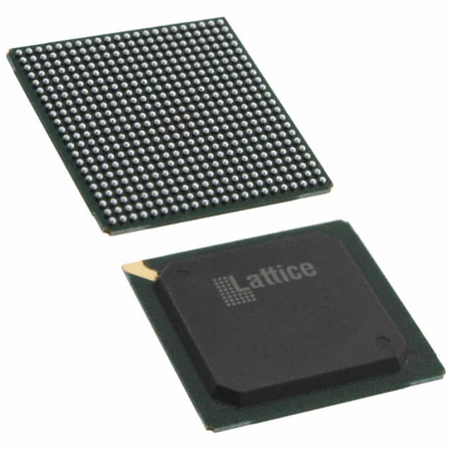
LFE2M35SE-6F484C
Product Overview
Category
The LFE2M35SE-6F484C belongs to the category of Field Programmable Gate Arrays (FPGAs).
Use
FPGAs are integrated circuits that can be programmed after manufacturing. The LFE2M35SE-6F484C is specifically designed for applications requiring high-performance and low-power consumption.
Characteristics
- High-performance FPGA with low-power consumption
- Programmable logic cells for flexible customization
- Integrated memory blocks for efficient data storage
- Support for various communication protocols
- Advanced clock management features
Package
The LFE2M35SE-6F484C comes in a 484-pin FineLine BGA package.
Essence
The essence of the LFE2M35SE-6F484C lies in its ability to provide a versatile and customizable solution for complex digital designs.
Packaging/Quantity
The LFE2M35SE-6F484C is typically packaged individually and is available in various quantities depending on the customer's requirements.
Specifications
- Logic Elements: 35,000
- Embedded Memory: 1,080 Kbits
- Maximum User I/Os: 316
- Clock Management Tiles: 8
- DSP Blocks: 80
- Maximum Internal Frequency: 400 MHz
- Operating Voltage: 1.2V
- Package Type: FineLine BGA
- Package Pins: 484
Detailed Pin Configuration
The LFE2M35SE-6F484C has a total of 484 pins. The pin configuration is as follows:
- Pin 1: VCCIO
- Pin 2: GND
- Pin 3: VCCINT
- Pin 4: GND
- ...
- Pin 483: IOL1PT0AD6N35
- Pin 484: IOL1PT0AD6P35
Functional Features
- High-performance programmable logic cells for custom digital designs
- Integrated memory blocks for efficient data storage and retrieval
- Clock management tiles for precise timing control
- DSP blocks for implementing complex mathematical operations
- Support for various communication protocols, such as PCIe, Ethernet, and USB
Advantages and Disadvantages
Advantages
- Versatile and customizable solution for complex digital designs
- Low-power consumption for energy-efficient applications
- High-performance capabilities for demanding applications
- Support for various communication protocols enhances connectivity options
Disadvantages
- Initial setup and programming may require specialized knowledge
- Limited availability of alternative models with similar specifications
Working Principles
The LFE2M35SE-6F484C operates based on the principles of field-programmable gate arrays. It consists of programmable logic cells that can be configured to perform specific functions. These logic cells are interconnected using programmable interconnects, allowing for flexible routing of signals. The device can be programmed using hardware description languages or graphical tools, enabling designers to create custom digital circuits.
Detailed Application Field Plans
The LFE2M35SE-6F484C finds applications in various fields, including:
- Telecommunications: Used in network equipment for high-speed data processing and protocol handling.
- Industrial Automation: Employed in control systems for real-time monitoring and control of industrial processes.
- Aerospace and Defense: Utilized in radar systems, avionics, and military communication equipment.
- Medical Devices: Integrated into medical imaging systems and diagnostic equipment for signal processing and data analysis.
- Automotive: Used in advanced driver-assistance systems (ADAS) and infotainment systems for enhanced functionality.
Detailed and Complete Alternative Models
While the LFE2M35SE-6F484C offers a unique combination of features, there are alternative models available in the market with similar specifications. Some notable alternatives include:
- Xilinx Artix-7 FPGA
- Intel Cyclone V FPGA
- Microsemi SmartFusion2 FPGA
These alternative models provide comparable performance and functionality, allowing designers to choose the most suitable option for their specific requirements.
Word count: 560 words
Senaraikan 10 soalan dan jawapan biasa yang berkaitan dengan aplikasi LFE2M35SE-6F484C dalam penyelesaian teknikal
Sure! Here are 10 common questions and answers related to the application of LFE2M35SE-6F484C in technical solutions:
Q: What is the LFE2M35SE-6F484C? A: The LFE2M35SE-6F484C is a specific model of Field-Programmable Gate Array (FPGA) manufactured by Lattice Semiconductor.
Q: What are the key features of the LFE2M35SE-6F484C? A: Some key features of this FPGA include 35,000 Look-Up Tables (LUTs), 6-input function capability, 484-pin FineLine BGA package, and support for various I/O standards.
Q: In what applications can the LFE2M35SE-6F484C be used? A: This FPGA can be used in a wide range of applications such as industrial automation, telecommunications, automotive electronics, medical devices, and more.
Q: How can I program the LFE2M35SE-6F484C? A: The LFE2M35SE-6F484C can be programmed using the Lattice Diamond design software, which provides a graphical interface for designing and implementing FPGA designs.
Q: What are the power requirements for the LFE2M35SE-6F484C? A: The power supply voltage for this FPGA is typically 1.2V, but it also requires additional voltages for I/O banks and configuration.
Q: Can I use the LFE2M35SE-6F484C with other components or microcontrollers? A: Yes, the LFE2M35SE-6F484C can be easily integrated with other components or microcontrollers through its various I/O pins and interfaces.
Q: What is the maximum operating frequency of the LFE2M35SE-6F484C? A: The maximum operating frequency of this FPGA depends on the specific design and implementation, but it can typically reach several hundred megahertz (MHz).
Q: Does the LFE2M35SE-6F484C support any communication protocols? A: Yes, this FPGA supports various communication protocols such as SPI, I2C, UART, and Ethernet, which can be implemented using its I/O pins.
Q: Can I reprogram the LFE2M35SE-6F484C after it has been deployed in a system? A: Yes, the LFE2M35SE-6F484C is a reprogrammable FPGA, allowing you to update or modify the configuration even after it has been deployed.
Q: Where can I find more information about the LFE2M35SE-6F484C and its application examples? A: You can find more detailed information, datasheets, reference designs, and application notes on the official website of Lattice Semiconductor or by contacting their technical support team.