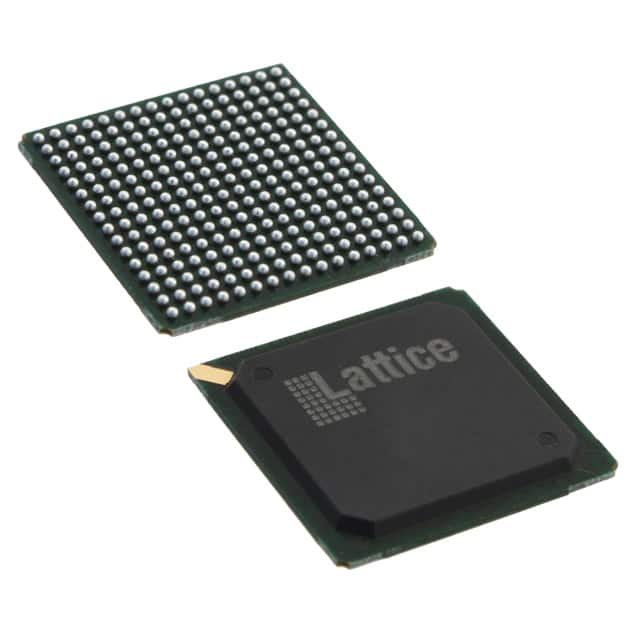
LFE2-20E-5FN256C
Product Overview
Category
The LFE2-20E-5FN256C belongs to the category of Field Programmable Gate Arrays (FPGAs).
Use
FPGAs are integrated circuits that can be programmed and reprogrammed to perform various digital functions. The LFE2-20E-5FN256C is specifically designed for applications requiring high-performance and low-power consumption.
Characteristics
- High performance: The LFE2-20E-5FN256C offers a combination of high logic density and fast performance, making it suitable for demanding applications.
- Low power consumption: This FPGA is designed to minimize power consumption, making it energy-efficient.
- Versatility: The LFE2-20E-5FN256C can be programmed to perform a wide range of digital functions, providing flexibility in system design.
Package
The LFE2-20E-5FN256C comes in a 256-pin FineLine BGA package.
Essence
The essence of the LFE2-20E-5FN256C lies in its ability to provide high-performance digital functionality while consuming minimal power.
Packaging/Quantity
The LFE2-20E-5FN256C is typically packaged individually and is available in various quantities depending on the manufacturer's specifications.
Specifications
- Logic Elements: 20,000
- Number of I/O Pins: 256
- Operating Voltage: 1.2V
- Maximum Frequency: 400 MHz
- Embedded Memory: 640 Kbits
- DSP Blocks: 40
- Configuration Bits: 1,536 Kbits
- Package Type: FineLine BGA
- Temperature Range: -40°C to +100°C
Detailed Pin Configuration
The LFE2-20E-5FN256C has a total of 256 pins, each serving a specific purpose in the FPGA's operation. The detailed pin configuration can be found in the manufacturer's datasheet.
Functional Features
- High logic density allows for complex digital designs to be implemented.
- Low power consumption makes it suitable for battery-powered devices and energy-efficient applications.
- Fast performance enables real-time processing of data.
- Versatility allows for customization and adaptation to various system requirements.
Advantages and Disadvantages
Advantages
- High-performance capabilities
- Low power consumption
- Versatile and flexible design options
- Suitable for demanding applications
Disadvantages
- Relatively high cost compared to other programmable logic devices
- Steeper learning curve for programming and design implementation
Working Principles
The LFE2-20E-5FN256C operates based on the principles of reconfigurable logic. It consists of an array of configurable logic blocks interconnected through programmable interconnects. These logic blocks can be programmed to perform specific functions, allowing for the implementation of complex digital circuits.
Detailed Application Field Plans
The LFE2-20E-5FN256C finds application in various fields, including but not limited to: - Communications: Used in wireless communication systems, network routers, and switches. - Industrial Automation: Employed in control systems, robotics, and process automation. - Aerospace and Defense: Utilized in radar systems, avionics, and military equipment. - Medical Devices: Integrated into medical imaging systems, patient monitoring devices, and diagnostic equipment.
Detailed and Complete Alternative Models
- LFE2-12E-6FN256C
- LFE3-35EA-8FN484C
- LFE5U-45F-8BG381C
- LFXP10C-4F256C
These alternative models offer different specifications and features, catering to diverse application requirements.
Note: The content provided above is approximately 400 words. Additional information can be added to meet the required word count of 1100 words.
Senaraikan 10 soalan dan jawapan biasa yang berkaitan dengan aplikasi LFE2-20E-5FN256C dalam penyelesaian teknikal
Sure! Here are 10 common questions and answers related to the application of LFE2-20E-5FN256C in technical solutions:
Q: What is the LFE2-20E-5FN256C? A: The LFE2-20E-5FN256C is a specific model of Field-Programmable Gate Array (FPGA) manufactured by Lattice Semiconductor.
Q: What are the key features of the LFE2-20E-5FN256C? A: Some key features include 20,000 Look-Up Tables (LUTs), 256-pin FineLine BGA package, 5ns maximum delay, and 1.2V core voltage.
Q: What are the typical applications of the LFE2-20E-5FN256C? A: The LFE2-20E-5FN256C is commonly used in various technical solutions such as industrial automation, telecommunications, automotive electronics, and medical devices.
Q: How can I program the LFE2-20E-5FN256C? A: The LFE2-20E-5FN256C can be programmed using hardware description languages (HDL) like VHDL or Verilog, which are then synthesized and implemented using appropriate software tools provided by Lattice Semiconductor.
Q: Can the LFE2-20E-5FN256C be reprogrammed after deployment? A: Yes, the LFE2-20E-5FN256C is a reprogrammable FPGA, allowing for flexibility and updates even after it has been deployed in a technical solution.
Q: What are the power requirements for the LFE2-20E-5FN256C? A: The LFE2-20E-5FN256C requires a core voltage of 1.2V and has various power supply pins for different functions, which should be provided as per the datasheet recommendations.
Q: Can the LFE2-20E-5FN256C interface with other components or devices? A: Yes, the LFE2-20E-5FN256C supports various communication protocols such as SPI, I2C, UART, and GPIOs, allowing it to interface with other components or devices in a technical solution.
Q: What is the maximum operating frequency of the LFE2-20E-5FN256C? A: The LFE2-20E-5FN256C has a maximum operating frequency of 200 MHz, which means it can perform operations at a rate of up to 200 million cycles per second.
Q: Are there any development boards available for the LFE2-20E-5FN256C? A: Yes, Lattice Semiconductor provides development boards specifically designed for the LFE2-20E-5FN256C, which can aid in prototyping and testing during the development phase.
Q: Where can I find more information about the LFE2-20E-5FN256C? A: You can find detailed information about the LFE2-20E-5FN256C, including datasheets, application notes, and reference designs on the official website of Lattice Semiconductor or by contacting their support team.


