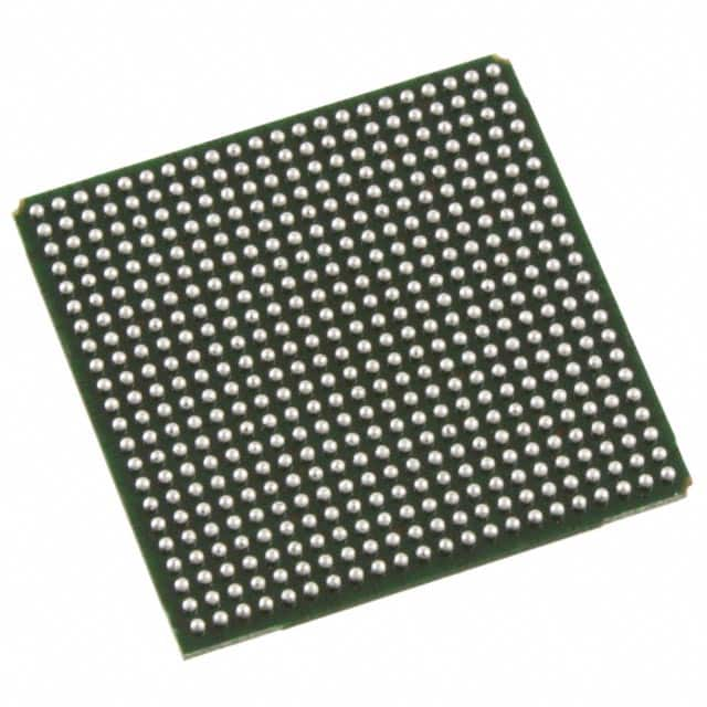
LFE2-12E-6F484C
Product Overview
Category
The LFE2-12E-6F484C belongs to the category of Field-Programmable Gate Arrays (FPGAs).
Use
This FPGA is commonly used in electronic circuits for various applications, including digital signal processing, data encryption, and high-speed communication systems.
Characteristics
- High-performance programmable logic device
- Low power consumption
- Flexible and reconfigurable design
- Fast processing speed
- Wide range of I/O interfaces
Package
The LFE2-12E-6F484C comes in a compact 484-pin FineLine BGA package.
Essence
The essence of this FPGA lies in its ability to provide a customizable hardware solution that can be programmed to perform specific functions according to the user's requirements.
Packaging/Quantity
Each package contains one LFE2-12E-6F484C FPGA.
Specifications
- Logic Elements: 12,000
- Flip-Flops: 6,000
- Embedded Memory: 648 Kbits
- Maximum User I/Os: 316
- Operating Voltage: 1.2V
- Operating Temperature Range: -40°C to 100°C
- Speed Grade: 6
Detailed Pin Configuration
The LFE2-12E-6F484C has a total of 484 pins, each serving a specific purpose in the circuit. The pin configuration includes input/output pins, power supply pins, clock pins, and configuration pins. For a detailed pinout diagram, please refer to the manufacturer's datasheet.
Functional Features
- Configurable logic blocks for implementing complex digital circuits
- Dedicated multipliers for efficient arithmetic operations
- High-speed I/O interfaces for seamless data transfer
- On-chip memory resources for storing intermediate results
- Built-in clock management resources for precise timing control
Advantages and Disadvantages
Advantages
- Versatile and adaptable to various applications
- Faster time-to-market due to programmable nature
- Lower development costs compared to custom ASICs
- Easy debugging and testing through reprogramming capability
Disadvantages
- Relatively higher power consumption compared to dedicated hardware solutions
- Limited performance compared to application-specific integrated circuits (ASICs)
- Higher cost per unit compared to mass-produced standard components
Working Principles
The LFE2-12E-6F484C FPGA operates based on the principles of configurable logic. It consists of an array of programmable logic elements interconnected by configurable routing resources. The user can program the FPGA using a Hardware Description Language (HDL) to define the desired circuit functionality. Upon configuration, the FPGA executes the programmed logic, enabling the desired operations.
Detailed Application Field Plans
The LFE2-12E-6F484C FPGA finds applications in various fields, including:
- Digital Signal Processing: Used for implementing complex algorithms in real-time audio and video processing systems.
- Communications: Enables high-speed data transmission and protocol handling in networking equipment.
- Industrial Automation: Provides customizable control and monitoring capabilities for industrial machinery and processes.
- Aerospace and Defense: Used in radar systems, avionics, and secure communication systems.
- Internet of Things (IoT): Facilitates the integration of multiple sensors and actuators in IoT devices.
Detailed and Complete Alternative Models
- LFE2-12E-5F484C: Similar to LFE2-12E-6F484C but with 5,000 logic elements.
- LFE2-12E-7F484C: Similar to LFE2-12E-6F484C but with 7,000 logic elements.
- LFE2-12E-6FN484C: Similar to LFE2-12E-6F484C but with additional DSP blocks for enhanced signal processing capabilities.
These alternative models offer different logic element counts and additional features to cater to specific application requirements.
In conclusion, the LFE2-12E-6F484C FPGA is a high-performance programmable logic device that offers flexibility, speed, and a wide range of applications. Its configurable nature allows for customization, making it a valuable component in various electronic systems.
Senaraikan 10 soalan dan jawapan biasa yang berkaitan dengan aplikasi LFE2-12E-6F484C dalam penyelesaian teknikal
Sure! Here are 10 common questions and answers related to the application of LFE2-12E-6F484C in technical solutions:
Q: What is the LFE2-12E-6F484C? A: The LFE2-12E-6F484C is a specific model of Field-Programmable Gate Array (FPGA) manufactured by Lattice Semiconductor.
Q: What are the key features of the LFE2-12E-6F484C? A: The key features of this FPGA include 12,000 Look-Up Tables (LUTs), 6 Input/Output Banks, and a 484-pin Fine-Pitch Ball Grid Array (FBGA) package.
Q: How can the LFE2-12E-6F484C be used in technical solutions? A: The LFE2-12E-6F484C can be used for various applications such as digital signal processing, embedded systems, communication protocols, and control systems.
Q: What programming languages can be used with the LFE2-12E-6F484C? A: The LFE2-12E-6F484C can be programmed using Hardware Description Languages (HDLs) like VHDL or Verilog.
Q: What development tools are available for working with the LFE2-12E-6F484C? A: Lattice provides software tools like Lattice Diamond or Lattice Radiant, which offer design entry, synthesis, simulation, and programming capabilities for this FPGA.
Q: Can the LFE2-12E-6F484C interface with other components or devices? A: Yes, the LFE2-12E-6F484C supports various standard interfaces such as SPI, I2C, UART, and GPIOs, allowing it to communicate with other components or devices.
Q: What is the power supply requirement for the LFE2-12E-6F484C? A: The LFE2-12E-6F484C typically operates at a voltage range of 1.14V to 1.26V, but it also requires additional voltages for I/O banks and configuration.
Q: Can the LFE2-12E-6F484C be reprogrammed after deployment? A: Yes, the LFE2-12E-6F484C is a reprogrammable FPGA, which means its configuration can be changed even after it has been deployed in a system.
Q: Are there any limitations or considerations when using the LFE2-12E-6F484C? A: Some considerations include power consumption, timing constraints, and resource utilization, which should be carefully managed during the design process.
Q: Where can I find more information about the LFE2-12E-6F484C? A: You can find detailed documentation, datasheets, application notes, and reference designs on the official website of Lattice Semiconductor or by contacting their support team.
Please note that the specific details and answers may vary depending on the context and requirements of your technical solution.


