

Encyclopedia Entry: 74FCT16952CTPVG
Product Information Overview
- Category: Integrated Circuit (IC)
- Use: Logic Level Translator
- Characteristics: High-speed, low-power consumption
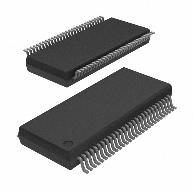
- Package: TSSOP (Thin Shrink Small Outline Package)
- Essence: Logic level translation between different voltage domains
- Packaging/Quantity: Tape and Reel, 2500 units per reel
Specifications
- Supply Voltage Range: 2.3V to 3.6V
- Input Voltage Range: 0V to VCC
- Output Voltage Range: 0V to VCC
- Operating Temperature Range: -40°C to +85°C
- Propagation Delay: 1.5ns (typical)
- Output Drive Capability: ±24mA
Detailed Pin Configuration
The 74FCT16952CTPVG IC has a total of 56 pins, which are organized as follows:
- Pin 1: GND (Ground)
- Pin 2: A1 (Input/Output)
- Pin 3: B1 (Input/Output)
- Pin 4: Y1 (Output)
- Pin 5: A2 (Input/Output)
- Pin 6: B2 (Input/Output)
- Pin 7: Y2 (Output)
- ...
- Pin 56: VCC (Supply Voltage)
Functional Features
- Logic Level Translation: The 74FCT16952CTPVG is designed to translate logic signals between different voltage domains.
- Bidirectional Operation: It supports bidirectional data flow, allowing translation in both directions.
- High-Speed Performance: With a propagation delay of only 1.5ns, it enables fast signal transmission.
- Low Power Consumption: The IC operates at low power levels, making it suitable for battery-powered devices.
Advantages and Disadvantages
Advantages: - Efficient Logic Level Translation: Enables seamless communication between devices operating at different voltage levels. - High-Speed Operation: Facilitates fast data transfer in various applications. - Compact Package: The TSSOP package offers a small footprint, ideal for space-constrained designs.
Disadvantages: - Limited Voltage Range: The IC is designed for voltage translation within the specified range and may not be suitable for extreme voltage differences. - Sensitivity to Noise: As with any high-speed IC, proper noise mitigation techniques should be employed to ensure reliable operation.
Working Principles
The 74FCT16952CTPVG utilizes a combination of level-shifting circuitry and bi-directional buffers to achieve logic level translation. It operates by detecting the input voltage levels and converting them to the corresponding output voltage levels based on the specified voltage ranges.
Detailed Application Field Plans
The 74FCT16952CTPVG can be used in various applications that require logic level translation, such as: 1. Microcontroller interfacing with different voltage peripherals. 2. Communication interfaces between systems operating at different voltage domains. 3. Signal conversion in mixed-voltage digital circuits. 4. Battery-powered devices requiring efficient voltage translation.
Detailed and Complete Alternative Models
- SN74LVC1T45DBVR: Single-Bit Dual-Supply Bus Transceiver
- TXB0108PWR: 8-Bit Bidirectional Voltage-Level Translator
- PCA9306DCUR: Dual Bidirectional I2C-Bus and SMBus Voltage-Level Translator
These alternative models offer similar functionality and can be considered as alternatives to the 74FCT16952CTPVG for logic level translation applications.
In conclusion, the 74FCT16952CTPVG is a high-speed logic level translator IC that enables seamless communication between devices operating at different voltage domains. Its compact package, low power consumption, and bidirectional operation make it suitable for a wide range of applications. However, designers should consider the voltage range limitations and employ proper noise mitigation techniques for reliable operation.
Senaraikan 10 soalan dan jawapan biasa yang berkaitan dengan aplikasi 74FCT16952CTPVG dalam penyelesaian teknikal
Sure! Here are 10 common questions and answers related to the application of 74FCT16952CTPVG in technical solutions:
Q: What is the function of the 74FCT16952CTPVG? A: The 74FCT16952CTPVG is a 16-bit registered transceiver with 3-state outputs, designed for high-speed data transmission.
Q: What is the operating voltage range of the 74FCT16952CTPVG? A: The operating voltage range of the 74FCT16952CTPVG is typically between 4.5V and 5.5V.
Q: Can the 74FCT16952CTPVG be used in both input and output applications? A: Yes, the 74FCT16952CTPVG can be used as both an input and output device, making it versatile for various technical solutions.
Q: What is the maximum data transfer rate supported by the 74FCT16952CTPVG? A: The 74FCT16952CTPVG supports high-speed data transfer rates up to 250 MHz.
Q: Does the 74FCT16952CTPVG have built-in ESD protection? A: Yes, the 74FCT16952CTPVG has built-in ESD protection, which helps safeguard against electrostatic discharge.
Q: Can the 74FCT16952CTPVG be cascaded with other devices? A: Yes, the 74FCT16952CTPVG can be cascaded with other similar devices to expand the number of inputs and outputs in a system.
Q: What is the power consumption of the 74FCT16952CTPVG? A: The power consumption of the 74FCT16952CTPVG is typically low, making it suitable for power-sensitive applications.
Q: Does the 74FCT16952CTPVG support hot insertion and removal? A: Yes, the 74FCT16952CTPVG supports hot insertion and removal, allowing for easy integration into existing systems.
Q: Can the 74FCT16952CTPVG operate in harsh environments? A: The 74FCT16952CTPVG has a wide operating temperature range and can withstand harsh environmental conditions.
Q: Are there any specific application notes or reference designs available for the 74FCT16952CTPVG? A: Yes, the manufacturer provides application notes and reference designs to assist with the implementation of the 74FCT16952CTPVG in various technical solutions.
Please note that the answers provided here are general and may vary depending on the specific requirements and datasheet of the 74FCT16952CTPVG.