

Encyclopedia Entry: 74FCT16543ATPVG8
Product Overview
Category
The 74FCT16543ATPVG8 belongs to the category of integrated circuits (ICs). Specifically, it falls under the category of octal registered transceivers.
Use
This product is primarily used for data transmission and reception between two separate buses. It enables bidirectional communication by converting signals from one bus into a compatible format for the other bus.
Characteristics
- Octal: The 74FCT16543ATPVG8 has eight channels, allowing for simultaneous transmission and reception of data.
- Registered: It incorporates flip-flops to store data temporarily, ensuring reliable and synchronized data transfer.
- Transceiver: This IC acts as both a transmitter and receiver, facilitating two-way communication between buses.
Package and Quantity
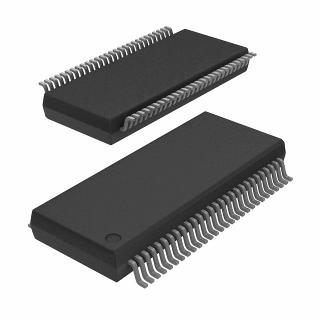
The 74FCT16543ATPVG8 is available in a standard 48-pin TSSOP (Thin Shrink Small Outline Package) package. Each package contains one unit of the IC.
Essence
The essence of the 74FCT16543ATPVG8 lies in its ability to enable efficient and reliable data transfer between two buses, making it an essential component in various electronic systems.
Specifications
- Supply Voltage: 4.5V to 5.5V
- Input/Output Voltage Range: 0V to VCC
- Operating Temperature Range: -40°C to +85°C
- Maximum Clock Frequency: 100MHz
- Output Drive Capability: ±24mA
Pin Configuration
The 74FCT16543ATPVG8 features a total of 48 pins, each serving a specific function. Here is a detailed pin configuration:
- Pin 1: Output Enable (OE)
- Pin 2: Data Input/Output (D0)
- Pin 3: Data Input/Output (D1)
- Pin 4: Data Input/Output (D2)
- Pin 5: Data Input/Output (D3)
- Pin 6: Data Input/Output (D4)
- Pin 7: Data Input/Output (D5)
- Pin 8: Data Input/Output (D6)
- Pin 9: Data Input/Output (D7)
- Pin 10: Clock (CLK)
- Pin 11: Output Enable (OE)
- Pin 12: Data Input/Output (D0)
- Pin 13: Data Input/Output (D1)
- Pin 14: Data Input/Output (D2)
- Pin 15: Data Input/Output (D3)
- Pin 16: Data Input/Output (D4)
- Pin 17: Data Input/Output (D5)
- Pin 18: Data Input/Output (D6)
- Pin 19: Data Input/Output (D7)
- Pin 20: Clock (CLK)
- Pin 21: GND (Ground)
- Pin 22: Data Input/Output (D8)
- Pin 23: Data Input/Output (D9)
- Pin 24: Data Input/Output (D10)
- Pin 25: Data Input/Output (D11)
- Pin 26: Data Input/Output (D12)
- Pin 27: Data Input/Output (D13)
- Pin 28: Data Input/Output (D14)
- Pin 29: Data Input/Output (D15)
- Pin 30: Clock (CLK)
- Pin 31: Output Enable (OE)
- Pin 32: Data Input/Output (D0)
- Pin 33: Data Input/Output (D1)
- Pin 34: Data Input/Output (D2)
- Pin 35: Data Input/Output (D3)
- Pin 36: Data Input/Output (D4)
- Pin 37: Data Input/Output (D5)
- Pin 38: Data Input/Output (D6)
- Pin 39: Data Input/Output (D7)
- Pin 40: Clock (CLK)
- Pin 41: Output Enable (OE)
- Pin 42: Data Input/Output (D0)
- Pin 43: Data Input/Output (D1)
- Pin 44: Data Input/Output (D2)
- Pin 45: Data Input/Output (D3)
- Pin 46: Data Input/Output (D4)
- Pin 47: Data Input/Output (D5)
- Pin 48: VCC (Supply Voltage)
Functional Features
Senaraikan 10 soalan dan jawapan biasa yang berkaitan dengan aplikasi 74FCT16543ATPVG8 dalam penyelesaian teknikal
Sure! Here are 10 common questions and answers related to the application of 74FCT16543ATPVG8 in technical solutions:
Q: What is the 74FCT16543ATPVG8? A: The 74FCT16543ATPVG8 is a 16-bit registered transceiver with 3-state outputs, designed for high-speed digital systems.
Q: What is the purpose of the 74FCT16543ATPVG8 in a technical solution? A: The 74FCT16543ATPVG8 can be used to enable bidirectional data transfer between two buses or systems.
Q: What is the maximum operating frequency of the 74FCT16543ATPVG8? A: The maximum operating frequency of the 74FCT16543ATPVG8 is typically specified by the manufacturer and can vary, but it is generally in the range of several hundred megahertz.
Q: How many input/output pins does the 74FCT16543ATPVG8 have? A: The 74FCT16543ATPVG8 has 16 input/output pins, corresponding to its 16-bit data width.
Q: Can the 74FCT16543ATPVG8 handle both TTL and CMOS logic levels? A: Yes, the 74FCT16543ATPVG8 is compatible with both TTL and CMOS logic levels, making it versatile for various applications.
Q: Does the 74FCT16543ATPVG8 support 3-state outputs? A: Yes, the 74FCT16543ATPVG8 has 3-state outputs, allowing for bus sharing and reducing contention issues.
Q: What is the power supply voltage range for the 74FCT16543ATPVG8? A: The 74FCT16543ATPVG8 typically operates with a power supply voltage range of 4.5V to 5.5V.
Q: Can the 74FCT16543ATPVG8 be used in high-speed data communication applications? A: Yes, the 74FCT16543ATPVG8 is designed for high-speed digital systems and can be used in applications requiring fast data transfer.
Q: Is the 74FCT16543ATPVG8 available in different package options? A: Yes, the 74FCT16543ATPVG8 is available in various package options, such as TSSOP, SSOP, and SOIC, to accommodate different design requirements.
Q: Are there any specific precautions to consider when using the 74FCT16543ATPVG8? A: It is important to follow the manufacturer's datasheet and guidelines for proper handling, power supply decoupling, and signal integrity considerations to ensure reliable operation of the 74FCT16543ATPVG8 in your technical solution.
Please note that the answers provided here are general and may vary depending on the specific implementation and manufacturer's specifications of the 74FCT16543ATPVG8.