

Encyclopedia Entry: 74AUP2G08RA3-7
Product Overview
Category
The 74AUP2G08RA3-7 belongs to the category of integrated circuits (ICs), specifically logic gates.
Use
This IC is commonly used in digital electronics for performing logical AND operations. It is designed to provide high-speed performance and low power consumption.
Characteristics
- High-speed operation: The 74AUP2G08RA3-7 is capable of operating at a high frequency, making it suitable for applications that require fast response times.
- Low power consumption: This IC is designed to minimize power consumption, making it ideal for battery-powered devices or energy-efficient systems.
- Small package size: The 74AUP2G08RA3-7 is available in a compact package, allowing for space-saving designs in electronic circuits.
- Wide supply voltage range: It can operate within a wide range of supply voltages, providing flexibility in various applications.
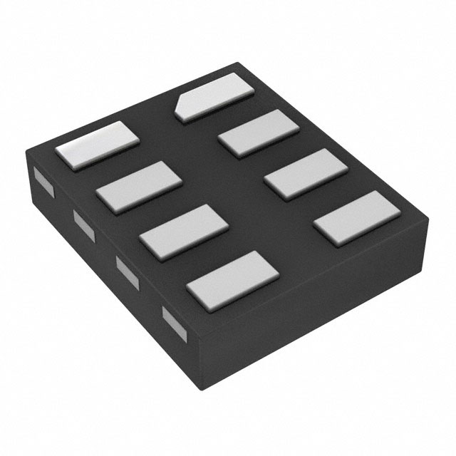
Package and Quantity
The 74AUP2G08RA3-7 is typically available in a small surface-mount package, such as a SOT-353 or XSON6 package. The exact package type may vary depending on the manufacturer. It is usually supplied in reels or tubes containing multiple units.
Specifications
- Supply Voltage Range: 0.8V to 3.6V
- Input Voltage Range: 0V to VCC
- Output Voltage Range: 0V to VCC
- Operating Temperature Range: -40°C to +85°C
- Logic Family: AUP
Pin Configuration
The 74AUP2G08RA3-7 has a total of 6 pins, which are assigned specific functions:
____
   Y1 --|    |-- VCC
   A1 --|    |-- B1
   GND --|    |-- Y2
        ------
Functional Features
The main functional feature of the 74AUP2G08RA3-7 is its ability to perform logical AND operations. It has two input pins (A1 and B1) and one output pin (Y1). The output pin provides a logic high (VCC) only when both input pins receive a logic high signal. Otherwise, the output remains at a logic low (GND).
Advantages and Disadvantages
Advantages
- High-speed operation allows for quick response times in digital circuits.
- Low power consumption makes it suitable for energy-efficient applications.
- Small package size enables space-saving designs.
- Wide supply voltage range provides flexibility in various systems.
Disadvantages
- Limited functionality: The 74AUP2G08RA3-7 is specifically designed for logical AND operations and may not be suitable for other types of logic functions.
- Sensitivity to voltage fluctuations: Care must be taken to ensure stable power supply conditions to prevent malfunctions.
Working Principles
The 74AUP2G08RA3-7 utilizes complementary metal-oxide-semiconductor (CMOS) technology to implement logical AND operations. It consists of transistors that switch between conducting and non-conducting states based on the input signals. When both input signals are high, the transistors allow current flow, resulting in a logic high output. If any of the inputs are low, the transistors block current flow, resulting in a logic low output.
Application Field Plans
The 74AUP2G08RA3-7 finds applications in various fields, including: 1. Digital communication systems 2. Microcontrollers and microprocessors 3. Consumer electronics 4. Automotive electronics 5. Industrial automation
Alternative Models
There are several alternative models available that can perform similar logical AND operations. Some popular alternatives to the 74AUP2G08RA3-7 include: - 74HC08: This IC operates at a higher voltage range and is compatible with TTL logic levels. - SN74LS08: A low-power Schottky version of the logical AND gate, suitable for applications requiring higher current drive capability.
These alternative models offer different specifications and features, allowing designers to choose the most appropriate option based on their specific requirements.
In conclusion, the 74AUP2G08RA3-7 is a high-speed, low-power logical AND gate integrated circuit. Its compact size, wide supply voltage range, and efficient performance make it a versatile choice for various digital electronics applications.
Word Count: 570
Senaraikan 10 soalan dan jawapan biasa yang berkaitan dengan aplikasi 74AUP2G08RA3-7 dalam penyelesaian teknikal
Sure! Here are 10 common questions and answers related to the application of the 74AUP2G08RA3-7 in technical solutions:
Q: What is the 74AUP2G08RA3-7? A: The 74AUP2G08RA3-7 is a dual 2-input AND gate integrated circuit (IC) that operates at a low voltage level.
Q: What is the operating voltage range of the 74AUP2G08RA3-7? A: The operating voltage range of the 74AUP2G08RA3-7 is typically between 0.8V and 3.6V.
Q: What is the maximum output current of the 74AUP2G08RA3-7? A: The maximum output current of the 74AUP2G08RA3-7 is around 32mA.
Q: Can the 74AUP2G08RA3-7 be used in battery-powered applications? A: Yes, the 74AUP2G08RA3-7 is suitable for battery-powered applications due to its low voltage operation.
Q: What is the propagation delay of the 74AUP2G08RA3-7? A: The propagation delay of the 74AUP2G08RA3-7 is typically around 2.5ns.
Q: Can the 74AUP2G08RA3-7 be used in high-speed applications? A: Yes, the 74AUP2G08RA3-7 can be used in high-speed applications due to its fast switching characteristics.
Q: Does the 74AUP2G08RA3-7 have built-in protection features? A: Yes, the 74AUP2G08RA3-7 has built-in ESD (electrostatic discharge) protection to prevent damage from static electricity.
Q: Can the 74AUP2G08RA3-7 be used in both digital and analog circuits? A: The 74AUP2G08RA3-7 is primarily designed for digital applications, but it can also be used in some low-frequency analog circuits.
Q: What is the package type of the 74AUP2G08RA3-7? A: The 74AUP2G08RA3-7 is available in a small SOT353 package.
Q: Are there any alternative ICs that can be used instead of the 74AUP2G08RA3-7? A: Yes, there are other similar dual 2-input AND gate ICs available in the market, such as the 74LVC2G08 or the SN74LVC2G08.