

S29GL064N90FFIS12
Product Overview
- Category: Flash Memory
- Use: Data storage and retrieval in electronic devices
- Characteristics: High capacity, fast read/write speeds, non-volatile memory
- Package: Integrated Circuit (IC)
- Essence: Non-volatile memory for reliable data storage
- Packaging/Quantity: Available in various packaging options, typically sold in bulk quantities
Specifications
- Model: S29GL064N90FFIS12
- Memory Type: NOR Flash
- Capacity: 64 Megabits (8 Megabytes)
- Operating Voltage: 2.7V - 3.6V
- Access Time: 90 nanoseconds
- Interface: Parallel
- Temperature Range: -40°C to +85°C
- Endurance: 100,000 program/erase cycles
- Data Retention: 20 years
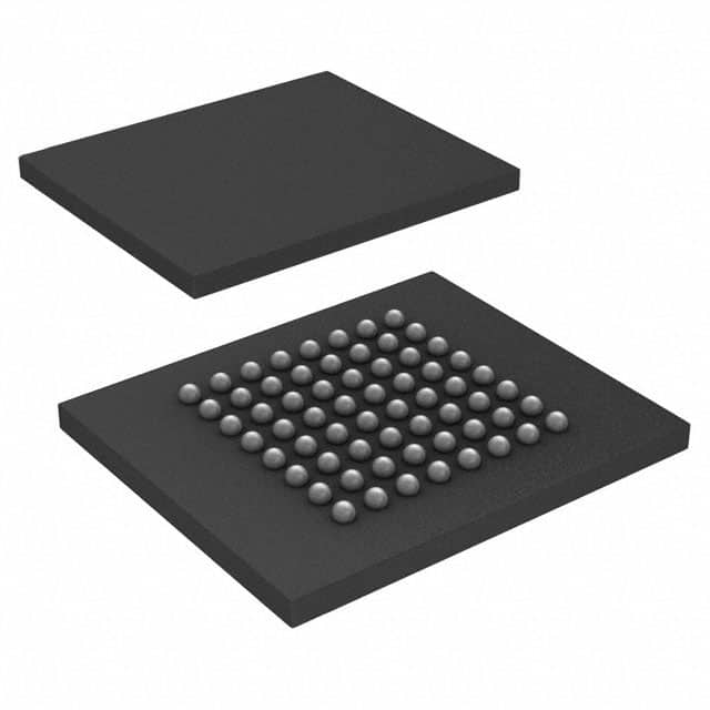
Pin Configuration (Detailed)
The S29GL064N90FFIS12 has a total of 48 pins arranged as follows:
- VCC (Power Supply)
- A0-A18 (Address Inputs)
- DQ0-DQ7 (Data Inputs/Outputs)
- WE# (Write Enable)
- CE# (Chip Enable)
- OE# (Output Enable)
- RP#/BYTE# (Reset/Byte Mode Select)
- RY/BY# (Ready/Busy)
- WP#/ACC (Write Protect/Acceleration)
- VSS (Ground)
(Note: Detailed pin configuration may vary depending on the package type.)
Functional Features
- High-speed read and write operations
- Sector erase capability for efficient memory management
- Built-in error correction codes (ECC) for data integrity
- Low power consumption during standby mode
- Hardware and software protection mechanisms for data security
Advantages
- Large storage capacity for storing extensive data
- Fast access times for quick data retrieval
- Reliable and durable non-volatile memory technology
- Suitable for a wide range of electronic devices and applications
- Efficient sector erase capability for flexible memory management
Disadvantages
- Higher cost compared to other types of memory
- Limited endurance in terms of program/erase cycles
- Requires additional circuitry for interfacing with microcontrollers
Working Principles
The S29GL064N90FFIS12 utilizes NOR flash memory technology, which is a type of non-volatile memory. It stores data by trapping electric charges within floating gate transistors. The presence or absence of charges determines the binary state of each memory cell.
During read operations, the memory controller sends an address to select a specific memory location. The stored data is then retrieved and sent back to the controller for further processing.
During write operations, the controller provides the address and data to be written. The memory cell at the specified address is erased (if necessary) and programmed with the new data.
Application Field Plans
The S29GL064N90FFIS12 is widely used in various electronic devices and applications, including:
- Embedded systems
- Automotive electronics
- Industrial control systems
- Consumer electronics
- Networking equipment
- Medical devices
Its high capacity, fast access times, and reliability make it suitable for storing firmware, operating systems, configuration data, and other critical information in these fields.
Alternative Models
- S29GL032N90FFIS12 - 32 Megabit (4 Megabyte) capacity
- S29GL128N90FFIS12 - 128 Megabit (16 Megabyte) capacity
- S29GL256N90FFIS12 - 256 Megabit (32 Megabyte) capacity
- S29GL512N90FFIS12 - 512 Megabit (64 Megabyte) capacity
(Note: The above models are just a few examples; there are several alternative models available with varying capacities and specifications.)
This concludes the encyclopedia entry for the S29GL064N90FFIS12 flash memory.
Senaraikan 10 soalan dan jawapan biasa yang berkaitan dengan aplikasi S29GL064N90FFIS12 dalam penyelesaian teknikal
Sure! Here are 10 common questions and answers related to the application of S29GL064N90FFIS12 in technical solutions:
Q: What is the S29GL064N90FFIS12? A: The S29GL064N90FFIS12 is a 64-megabit (8 megabyte) flash memory device manufactured by Cypress Semiconductor.
Q: What are the key features of the S29GL064N90FFIS12? A: Some key features include a 90 nanosecond access time, a 3V power supply, a 128-word buffer for programming, and a high endurance of 100,000 program/erase cycles.
Q: What are some typical applications of the S29GL064N90FFIS12? A: The S29GL064N90FFIS12 is commonly used in various applications such as embedded systems, automotive electronics, industrial control systems, and consumer electronics.
Q: How can I interface with the S29GL064N90FFIS12? A: The S29GL064N90FFIS12 supports a standard parallel interface, making it compatible with many microcontrollers and processors.
Q: What is the maximum operating frequency of the S29GL064N90FFIS12? A: The S29GL064N90FFIS12 can operate at frequencies up to 66 MHz, allowing for fast data transfer rates.
Q: Can the S29GL064N90FFIS12 be easily soldered onto a PCB? A: Yes, the S29GL064N90FFIS12 comes in a standard surface-mount package, making it easy to solder onto a printed circuit board.
Q: Does the S29GL064N90FFIS12 support hardware and software data protection? A: Yes, the S29GL064N90FFIS12 provides both hardware and software data protection features to prevent unauthorized access or modification.
Q: What is the typical power consumption of the S29GL064N90FFIS12? A: The S29GL064N90FFIS12 has a low power consumption, typically drawing around 30 mA during active operation and less than 1 µA in standby mode.
Q: Can the S29GL064N90FFIS12 withstand harsh environmental conditions? A: Yes, the S29GL064N90FFIS12 is designed to operate reliably in a wide temperature range (-40°C to +85°C) and can withstand high levels of shock and vibration.
Q: Are there any development tools or resources available for working with the S29GL064N90FFIS12? A: Yes, Cypress Semiconductor provides various development tools, datasheets, application notes, and technical support to assist engineers in designing with the S29GL064N90FFIS12.
Please note that the answers provided here are general and may vary depending on specific requirements and use cases.