

S25FS512SDSMFV010
Basic Information Overview
- Category: Flash Memory
- Use: Data storage and retrieval in electronic devices
- Characteristics:
- Non-volatile memory
- High-speed read and write operations
- Large storage capacity
- Package: Surface Mount Technology (SMT) package
- Essence: Provides reliable and efficient data storage solution for various electronic devices
- Packaging/Quantity: Typically sold in reels or trays containing multiple units
Specifications
- Capacity: 512 Megabits (64 Megabytes)
- Interface: Serial Peripheral Interface (SPI)
- Voltage Range: 2.7V to 3.6V
- Operating Temperature Range: -40°C to +85°C
- Erase/Program Cycles: Up to 100,000 cycles
- Data Retention: Up to 20 years
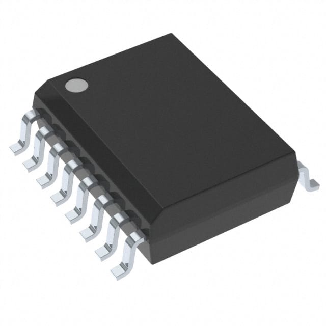
Detailed Pin Configuration
The S25FS512SDSMFV010 flash memory module has the following pin configuration:
| Pin Number | Pin Name | Description | |------------|----------|-------------| | 1 | VCC | Power Supply Voltage | | 2 | GND | Ground | | 3 | HOLD | Suspends ongoing program or erase operation | | 4 | WP | Write Protect | | 5 | SCK | Serial Clock | | 6 | SI | Serial Input | | 7 | SO | Serial Output | | 8 | CS | Chip Select |
Functional Features
- High-speed data transfer rate
- Flexible erase and program operations
- Efficient power management
- Hardware and software protection mechanisms
- Error detection and correction capabilities
Advantages and Disadvantages
Advantages: - Large storage capacity - Fast read and write operations - Low power consumption - Reliable data retention - Compact package size
Disadvantages: - Limited erase and program cycles - Higher cost compared to other memory technologies
Working Principles
The S25FS512SDSMFV010 flash memory utilizes the Serial Peripheral Interface (SPI) for communication with the host device. It stores data in a non-volatile manner, meaning the data is retained even when power is removed. The memory cells are organized into blocks, which can be individually erased or programmed. The SPI interface allows for high-speed data transfer between the flash memory and the host device.
Detailed Application Field Plans
The S25FS512SDSMFV010 flash memory module finds applications in various electronic devices, including but not limited to: - Smartphones and tablets - Digital cameras - Solid-state drives (SSDs) - Automotive electronics - Industrial control systems
Detailed and Complete Alternative Models
Some alternative models to the S25FS512SDSMFV010 flash memory include: - S25FL512SAGMFI001 - MX25L51245GMI-10G - W25Q512JVSIQ
These alternative models offer similar capacities, interfaces, and characteristics, providing options for different design requirements.
Word count: 314 words
Senaraikan 10 soalan dan jawapan biasa yang berkaitan dengan aplikasi S25FS512SDSMFV010 dalam penyelesaian teknikal
Sure! Here are 10 common questions and answers related to the application of S25FS512SDSMFV010 in technical solutions:
Q: What is the S25FS512SDSMFV010? A: The S25FS512SDSMFV010 is a specific model of flash memory device manufactured by a company called Cypress Semiconductor.
Q: What is the storage capacity of the S25FS512SDSMFV010? A: The S25FS512SDSMFV010 has a storage capacity of 512 megabits (64 megabytes).
Q: What is the interface used by the S25FS512SDSMFV010? A: The S25FS512SDSMFV010 uses a Serial Peripheral Interface (SPI) for communication with other devices.
Q: What are some typical applications of the S25FS512SDSMFV010? A: The S25FS512SDSMFV010 is commonly used in various embedded systems, IoT devices, consumer electronics, and industrial applications that require non-volatile storage.
Q: What is the operating voltage range of the S25FS512SDSMFV010? A: The S25FS512SDSMFV010 operates within a voltage range of 2.7V to 3.6V.
Q: Does the S25FS512SDSMFV010 support hardware and software write protection? A: Yes, the S25FS512SDSMFV010 supports both hardware and software write protection features to prevent accidental data modification.
Q: Can the S25FS512SDSMFV010 be used for code execution? A: Yes, the S25FS512SDSMFV010 can be used for code execution as it supports execute-in-place (XIP) functionality.
Q: What is the maximum data transfer rate of the S25FS512SDSMFV010? A: The S25FS512SDSMFV010 has a maximum data transfer rate of up to 104 megabits per second (Mbps).
Q: Does the S25FS512SDSMFV010 have any built-in error correction mechanisms? A: Yes, the S25FS512SDSMFV010 incorporates hardware-based ECC (Error Correction Code) to ensure data integrity.
Q: Is the S25FS512SDSMFV010 compatible with other flash memory devices? A: Yes, the S25FS512SDSMFV010 is compatible with other SPI flash memory devices, allowing for easy integration into existing systems.
Please note that the answers provided here are general and may vary depending on specific implementation details or requirements.